Add to Cart
Automotive navigation board chip processing is a precise and
critical manufacturing process, its process covers a number of
rigorous steps.
The first is the solder paste printing link, the high-precision
solder paste press will paste evenly on the solder pad of the
circuit board. This step requires the press to accurately control
the thickness, position and amount of the solder paste, because the
state of the solder paste directly affects the subsequent welding
quality.
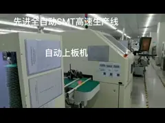
Next is the placement process, the advanced placement machine
according to the pre-set program, from the feeder to grab resistor,
capacitor, chip and other small surface mount components, and then
placed them in the solder paste coated circuit board with high
precision. The speed and positioning accuracy of the mounter are
crucial to ensure that each component can be correctly placed.
After the placement is completed, the reflow welding stage is
entered, and the circuit board containing the components is fed
into the reflow furnace. The furnace is heated according to a
specific temperature curve, the solder paste is heated and melted,
and the components and the circuit board are solidly welded
together. Precise control of temperature and time is the key to
this link, too high temperature or too long time may damage the
components, otherwise it will lead to poor welding.
The final part is the inspection process, through automatic optical
inspection (AOI) equipment to conduct a comprehensive inspection of
the welded motherboard, identifying welding defects such as missing
parts, offset, short circuit and so on. For the detected problem
products, manual repair or rework processing will be carried out to
ensure that each piece of the vehicle navigator motherboard meets
high quality standards, providing reliable protection for
subsequent installation and use.