
Add to Cart
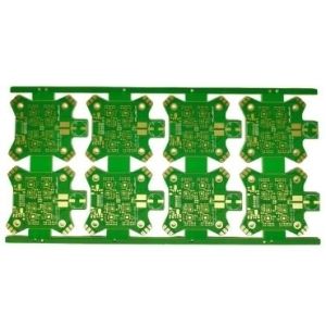
Best Price16 Layers Prototype Board HDI Multilayer PCB
♦ What is HDI PCBs?
HDI PCB (High-Density Interconnect Printed Circuit Board) is a circuit board built with very fine lines/spaces (≤ 100 µm), micro-vias (≤ 150 µm), blind/buried vias, and often sequential lamination or laser-drilled stacked vias, so that more components and routing can fit in a smaller area. The result is thinner, lighter boards with higher I/O counts, shorter signal paths and better electrical performance—ideal for smartphones, tablets, medical implants, IoT modules and any application demanding miniaturization and high speed.
♦ Technical Parameters
Item | Spec |
Layers | 1~64 |
Board Thickness | 0.1mm-10 mm |
Material | FR-4, CEM-1/CEM-3, PI, High Tg, Rogers, PTEF, Alu/Cu Base,Ceramic, etc |
Max Panel Size | 800mm×1200mm |
Min Hole Size | 0.075mm |
Min Line Width/Space | Standard: 3mil(0.075mm) Advance: 2mil |
Board Outline Tolerance | 士0.10mm |
Insulation Layer Thickness | 0.075mm--5.00mm |
Out Layer Copper Thickness | 18um--350um |
Drilling Hole (Mechanical) | 17um--175um |
Finish Hole (Mechanical) | 17um--175um |
Diameter Tolerance (Mechanical) | 0.05mm |
Registration (Mechanical) | 0.075mm |
Aspect Ratio | 17:01 |
Solder Mask Type | LPI |
SMT Min. Solder Mask Width | 0.075mm |
Min. Solder Mask Clearance | 0.05mm |
Plug Hole Diameter | 0.25mm--0.60mm |


