Product Details
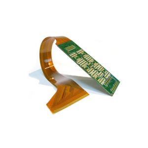
4 Layer PCB Flexible Board for Medical Device
♦ What is 4 Layer PCB?
A 4-layer PCB is a printed circuit board with four conductive
copper layers stacked together with insulating (dielectric)
material in between. These layers are interconnected through
vias (plated holes) to create complex circuits while saving
space and improving performance compared to single or double-sided
boards.
♦ Structure of a 4-Layer PCB
A typical 4-layer stackup consists of:
- Top Layer (Signal Layer) – Contains component placements and
high-speed signal traces.
- Inner Layer 1 (Ground Plane) – Acts as a reference plane for
EMI shielding and noise reduction.
- Inner Layer 2 (Power Plane) – Distributes stable power supply
to components.
- Bottom Layer (Signal Layer) – Additional routing space for
signals and components.
♦ 4-Layer PCB vs. 2-Layer PCB
| Feature | 4-Layer PCB | 2-Layer PCB |
|---|
| Layers | 4 (Signal+GND+PWR) | 2 (Top+Bottom) |
| Routing Space | ✅ High | ❌ Limited |
| Signal Noise | ✅ Low (GND plane) | ❌ Higher |
| EMI Shielding | ✅ Better | ❌ Poor |
| Cost | ⚠️ Higher (~2x) | ✅ Lower |
♦ Manufacturing Process
- Design – Use CAD tools (Altium, KiCad) to define layer stackup and
routing.
- Material Selection – Choose core/prepreg materials (FR-4, Rogers).
- Lamination – Bond layers under heat/pressure.
- Drilling & Plating – Create vias for inter-layer connections.
- Etching – Remove excess copper to form traces.
- Testing – Verify continuity, impedance, and shorts.
♦ Technical Parameters
Item | Spec |
Layers | 1~64 |
Board Thickness | 0.1mm-10 mm |
Material | FR-4, CEM-1/CEM-3, PI, High Tg, Rogers, PTEF, Alu/Cu Base,Ceramic, etc |
Max Panel Size | 800mm×1200mm |
Min Hole Size | 0.075mm |
Min Line Width/Space | Standard: 3mil(0.075mm) Advance: 2mil |
Board Outline Tolerance | 士0.10mm |
Insulation Layer Thickness | 0.075mm--5.00mm |
Out Layer Copper Thickness | 18um--350um |
Drilling Hole (Mechanical) | 17um--175um |
Finish Hole (Mechanical) | 17um--175um |
Diameter Tolerance (Mechanical) | 0.05mm |
Registration (Mechanical) | 0.075mm |
Aspect Ratio | 17:01 |
Solder Mask Type | LPI |
SMT Min. Solder Mask Width | 0.075mm |
Min. Solder Mask Clearance | 0.05mm |
Plug Hole Diameter | 0.25mm--0.60mm |
Company Profile
DQS Electronic is located in Shenzhen, focusing on PCB Layout Design, PCB
Fabrication, Electronic Components Sourcing, SMT, PCB Assembly and
Testing. We are a one-stop EMS electronic manufacturing company
committed to providing global customers with rapid prototyping and
mass production.
Our products include single, double, multi, high frequency,
aluminum base, copper base, FR-4 and other high precision circuit
boards.
We have over 10 years of experience in serving many domestic and
foreign brand customers in a wide range of fields such as Medical,
Automotive, Industrial Automation, Artificial Intelligence, Smart
Home, Security, Power and Communications, etc..