Terrene Trading Limited is established in 2014, functions as a
buying office in China, and joined ZCF Group since January 2017.
The head office is allocated in Shenzhen China, the biggest PCB
related production base in China, belongs to High-Tech Industry
that collects Technology, R&D, Production and Sales. Terrene
started to develop an oversea branch in Taiwan Shinchu for
servicing more customers around the world.
Terrene offers one stop service for customers oversea who need
someone trustworthy to help them to search, purchase and integrate
the goods they want. Terrene can save you plenty of time and
energy, minimize the purchasing cost and offer the right products
you need. This high efficient working way will promote your
business development greatly.
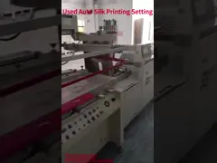
Terrene mainly concentrates on exporting 2nd hand PCB industrial
equipments, PCB consumptive materials, PCB machines parts for PCB
industry. Terrene can help to arrange and search second hand
machines based on customers' requests.
Since been established, Terrene has insisted on talent oriented
base, credibility as the management principle, gathering elites
from different areas, collecting advanced news, technologies,
management methods of enterprise experiences from overseas,
specifically combining the information with enterprises in China,
offering overall solution plans, helping enterprises to enhance
management level and production capabilities, making enterprises
keep competitive strength in this fierce competitive market,
achieving enterprises to develop rapidly and stably.
For developing the products that really suitable for enterprises
needs.
Terrene follows closely with PCB related techniques and industrial
development figures, continuously optimizes and develops new
products, and helps the enterprises to have superior services and
best investment rewords.
Terrence will offer enterprises the best products, the best
whole-set services, with the best reputations. Terrene are willing
to be your reliable long-term partner.