
Add to Cart
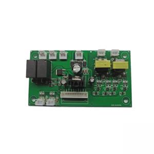
Testability PCB Manufacturing Hard Disk Pcb Board Industrial Control
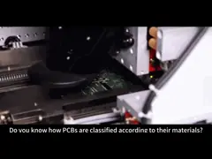
PCB Manufacturing Introduce:
PCB and PCBA, as important components in the electronics industry,
play a key role in electrical interconnection and circuit support.
It is widely used in industrial control, communication modules,
medical, automotive electronics, security equipment, and other
industries. PCB printed circuit board provides the fixing and
electrical connection of electronic components, while PCBA, as the
processing process of the printed circuit board, completes the
assembly and welding of components.
PCB Manufacturing Parameters:
| Item | Technical Parameter |
| Layer | 2-64 |
| Thickness | 0.3-6.5mm |
| Copper Thickness | 0.3-12 oz |
| Min Mechanical Hole | 0.1mm |
| Min Laser Hole | 0.075mm |
| HDI | 1+n+1,2+n+2,3+n+3 |
| Max Aspect Ratio | 20:01 |
| Max Board Size | 650mm*1130mm |
| Min Width/Space | 2.4/2.4mil |
| Min Outline Tolerance | ±0.1mm |
| Impedance Tolerance | ±5% |
| Min PP Thickness | 0.06mm |
| Bow &Twist | ≤0.5% |
| Materials | FR4, High-Tg FR4, Rogers, Nelco, RCC, PTFE, M4, M6, TU862, TU872 |
| Surface Finished | HASL, HASL Pb Free Immersion Gold/Tin/Silver Osp, Immersion Gold+OSP |
| Special Capability | Gold Finger Plating, Peelable, Carbon ink |
PCB Manufacturing FAQ:
Q1: What is the surface treatment material for PCB assembly?
A1: Spray tin, spray tin lead-free immersion gold/tin/Silver Gold
Finger Plating OSP, immersion gold + OSP.
Q2: What are the special capabilities of printed circuit board
assembly?
A2: Gold finger, peelable, carbon ink.