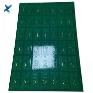
10 Layers PCB Quick Turn Printed Circuit Boards Fr4 Material For Airplane
Brand Name:YScircuit
Certification:ISO9001,UL,REACH, RoHS
Model Number:YS-ML-0005
Minimum Order Quantity:1 piece
Delivery Time:2-8 days
Payment Terms:T/T,PayPal, Alibaba pay
Contact Now
Add to Cart
Verified Supplier
Location:
Shenzhen China
Address:
Shenzhen YingSheng Technology Co., Ltd 805, Tongxin Technology Building, Qiaotou Community, Fuhai Street, Baoan District, Shenzhen
Supplier`s last login times:
within 34 hours
Shipping
lt's easy to get a shipping quote! Just click the button below and complete the short form.
Get Shipping Quote
Product Details
Company Profile
Product Details
10 Layers Pcb Quick Turn Fr4 Print Circuit Boards For Airplane
What is a quick turn PCB?
Getting electronic products to market depends on rapid manufacturing capabilities.
A quick turn PCB is critical during the prototype, pre-production, and full production phases of any product containing a printed circuit board.
Inconsistent timelines can lead to product delays and rushed testing, ultimately resulting in a poorer quality product.
YScircuit offers quick turn PCBs with quality in mind. We look at quick turn PCB manufacturing throughout each stage of the process, and provide realistic timelines for different sizes of orders.
| layer/m² | S<1㎡ | S<3㎡ | S<6㎡ | S<10㎡ | S<13㎡ | S<16㎡ | S<20㎡ | S<30㎡ | S<40㎡ | S<50㎡ | S<65㎡ | S<85㎡ | S<100㎡ |
| 1L | 4wds | 6wds | 7wds | 7wds | 9wds | 9wds | 10wds | 10wds | 10wds | 12wds | 14wds | 15wds | 16wds |
| 2L | 4wds | 6wds | 9wds | 9wds | 11wds | 12wds | 13wds | 13wds | 15wds | 15wds | 15wds | 15wds | 18wds |
| 4L | 6wds | 8wds | 12wds | 12wds | 14wds | 14wds | 14wds | 14wds | 15wds | 20wds | 25wds | 25wds | 28wds |
| 6L | 7wds | 9wds | 13wds | 13wds | 17wds | 18wds | 20wds | 22wds | 24wds | 25wds | 26wds | 28wds | 30wds |
| 8L | 9wds | 12wds | 15wds | 18wds | 20wds | 20wds | 22wds | 24wds | 26wds | 27wds | 28wds | 30wds | 30wds |
| 10L | 10wds | 13wds | 17wds | 18wds | 20wds | 20wds | 22wds | 24wds | 26wds | 27wds | 28wds | 30wds | 30wds |
| 12L | 10wds | 15wds | 17wds | 18wds | 20wds | 20wds | 22wds | 24wds | 26wds | 27wds | 28wds | 30wds | 30wds |
| 14L | 10wds | 16wds | 17wds | 18wds | 20wds | 20wds | 22wds | 24wds | 26wds | 27wds | 28wds | 30wds | 30wds |
| 16L | 10wds | 16wds | 17wds | 18wds | 20wds | 20wds | 22wds | 24wds | 26wds | 27wds | 28wds | 30wds | 30wds |
| 0-0.5m2 | 0.5-1m2 | 1-3m2 | 3-5m2 | 5-10m2 | |
| 1-2L | 24H | 24H | 3wds | 4wds | 5wds |
| 4L | 24H | 48H | 4wds | 5wds | 6wds |
| 6L | 48H | 48H | 4wds | 6wds | 6wds |
| 8L | 48H | 36H | 5wds | 6wds | 8wds |
YScircuit PCB Capabilities
Tolerance
What is Multilayer PCBs
Multilayer Printed Circuit Board, It is a type of PCB which comes with a combination of single sided PCB and double sided PCB.
It features layers more than double sided PCB.
PCB Sideplating
Sideplating is the metalization of the board edge in the PCB filed.
Edge plating, Border plated, plated contour, side metal, these words can also be used to describe the same function.
Half-cut Castellated Holes
Castellations are plated through holes or vias located in the edges of a printed circuit board.
Are indentations created in the form of semi-plated holes on the edges of the PCB boards.
These half holes serve as pads intended to create a link between the module board and the board that it will be soldered onto.
Parameters
- Layers: 10L multilayer pcb
- Board Thinkness:2.0mm
- Base Material:S1000-2 High tg
- Min Holes:0.2mm
- Minimum Line Width/Clearance:0.25mm/0.25mm
- Minimum Clearance between Inner Layer PTH to Line: 0.2mm
- Size:250.6mm×180.5mm
- Aspect Ratio:10 : 1
- Surface treatment:ENIG+ Selective hard gold
- Process characteristics: High tg, Sideplating, Selective hard gold, Half-cut Castellated Holes
- Applications: Wi-Fi modules
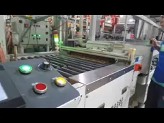
YScircuit Print Circuit Boards Production Process
PCB Stack UP
FQA
1. What is hard gold in PCB?
The Hard Gold surface finish, also known as Hard Electrolytic Gold, is composed of a layer of gold with added hardeners for increased durability, plated over a barrier coat of nickel using an electrolytic process.
2. What is hard gold plating?
Hard gold plating is a gold electrodeposit that has been alloyed
with another element to alter the grain structure of the gold to
achieve a harder deposit with a more refined grain structure.
The most common alloying elements used in hard gold plating are cobalt, nickel or iron.
3. What is the difference between Enig and hard gold?
ENIG plating is much softer than hard gold plating.
Grain sizes are about 60 times larger with ENIG plating, and hardness runs between 20 and 100 HK25.
ENIG plating holds up well at only 35 grams of contact force or less, and ENIG plating typically lasts for fewer cycles than hard plating.
A popular trend among manufacturers is board-to-board soldering.
This technique allows companies to produce integrated modules (often containing dozens of parts) on a single board that can be built into another assembly during production.
One easy way to produce a PCB that is destined to be mounted to another PCB is to create castellated mounting holes.
These are also known as "castellated vias" or "castellations."


10 Layers PCB Quick Turn Printed Circuit Boards Fr4 Material For Airplane
Inquiry Cart
0