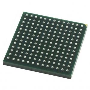
GW1N-UV9UG169C6 I5 Field Programmable Gate Array FPGA UBGA-169

Brand Name:GOWIN Semiconductor
Model Number:GW1N-UV9UG169C6/I5
Minimum Order Quantity:50pcs
Price:Negotiable
Supply Ability:1000000pcs
Number of Logic Elements:8640 LE
Contact Now

Add to Cart

Verified Supplier
Location: Shenzhen China
Address: Room 3001-2, Tower A, World Trade Plaza, No. 9 Fuhong Road, Futian District, Shenzhen
Supplier`s last login times: within 23 hours
Product Details Company Profile
Product Details

GW1N-UV9UG169C6/I5 FPGA - Field Programmable Gate Array

GOWIN LittleBee® GW1N-9 FPGAs

GOWIN Semiconductor LittleBee® GW1N-9 FPGAs provide a generous amount of logic resources, multiple I/O standards, embedded BSRAM, DSP, PLL, and built-in flash. The non-volatile FPGAs have many desirable options, including low power, instant-start, low-cost, high-security, a small size, variety of packages, and flexible usage.

The GOWIN Semiconductor GW1N-9 FPGAs are part of the LittleBee family of devices. LittleBee products are based on 55nm LP technology and offer instant-on, non-volatile, low power, intensive I/O, and a small footprint (smallest being 2.4mm x 2.3mm). The LittleBee family is ideal for high-performance bridging applications and supports MIPI I3C and MIPI D-PHY as standard. This support further reduces the board space and enhances performance.

The GW1N-9 apply FPGA synthesizing, layout, place and routing, data bitstream generation, and downloads through GOWIN Semi's FPGA hardware development environment.

FEATURES

  • User Flash
    • Up to 608Kbits
    • 10,000 write cycles
  • Lower power consumption
    • 55nm embedded flash technology
    • UV - Supports same power supply for VCC/ VCCO/ VCCx
    • Clock dynamically turns on and off
  • Multiple I/O standards
    • LVCMOS33/25/18/15/12; LVTTL33, SSTL33/25/18 I, SSTL33/25/18 II, SSTL15; HSTL18 I, HSTL18 II, HSTL15 I; PCI, LVDS25, RSDS, LVDS25E, BLVDSE, MLVDSE, LVPECLE, RSDSE
    • Input hysteresis option
    • Supports 4mA, 8mA, 16mA, 24mA, etc. drive options
    • Slew rate option
    • Output drive strength option
    • Individual Bus Keeper, Weak Pull-up, Weak Pull-down, and Open Drain option
    • Hot socket
  • High Performance DSP
    • High performance digital signal processing ability
    • Supports 9 x 9, 18 x 18, 36 x 36bit multiplier and 54bit accumulator
    • Multipliers cascading
    • Registers pipeline and bypass
    • Adaptive filtering through signal feedback
    • Supports barrel shifter
  • Abundant Slices
    • 4 input LUT (LUT4)
    • Double-edge flip-flops
    • Supports shift register and distributed register
  • Block SRAM with multiple modes
    • Supports dual port, single port, and semi dual port
    • Supports bytes write enable
  • Flexible PLLs
    • Frequency adjustment (multiply and division) and phase adjustment
    • Supports global clock
  • Built-in flash programming
    • Instant-on
    • Supports security bit operation
    • Supports AUTO BOOT and DUAL BOOT
  • Configuration
    • JTAG configuration
    • Up to 6 GowinCONFIG configuration modes - AUTOBOOT, SSPI, MSPI, CPU, SERIAL, DUAL BOOT

APPLICATIONS

  • Embedded
  • Server

SPECIFICATIONS CHART

PINOUT

SECUREFPGA DEVICE DIAGRAM

China GW1N-UV9UG169C6 I5 Field Programmable Gate Array FPGA UBGA-169 supplier

GW1N-UV9UG169C6 I5 Field Programmable Gate Array FPGA UBGA-169

Inquiry Cart 0