Product Details
custom pcb board design, pcb layout design services, electrical
circuits
Essential details
- Model Number:
PCB
- Place of Origin:
Guangdong, China
- Brand Name:
JIETENG
- Number of Layers:
4 Layer
- Base Material:
FR4
- Copper Thickness:
1oz
- Board Thickness:
1.6mm
- Min. Hole Size:
4mil
- Min. Line Width:
4mil
- Min. Line Spacing:
6mil
- Surface Finishing:
HASL
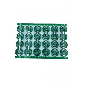
- Board Size:
123*108mm
- Max. panel size (finished) (mm):
880*580
- Max. working panel size (mm):
914*602
- Max. board thickness (mm):
12
- Max. layer-up(L):
40
- Aspect:
30:1(Min. hole:0.4mm)
- Line wide/space (mm):
0.075/0.075
- Back drill capability:
Yes
- Tolerance of back drill (mm):
±0.05
- Tolerance of press fit holes (mm):
±0.05
- Surface treatment type:
OSP,sterling silver,ENIG
Layer | 1~64 Layers |
Material | FR4, CEM1, CEM3, Hight TG, Rogers, F4B, Taconic, FR1, FR2, 94V0,
Aluminum |
Production Capacity | 30000 ㎡/months |
Board shape | Rectangular, Round, Slots, Cutouts, Complex Irregular |
Board cutting | Shear, V-Score, Tab-Routed, Counter Sunk |
Board thickness | 0.2~8.0mm, Flex 0.1-0.25mm |
Copper weight | 0.5oZ~12oZ |
Solder Mask | Double-sided Green LPI, Red, White, Yellow, Blue, Black, Purple
etc.Solder mask |
Silk screen | Double-Sided or Single-Sided in White, Yellow, Black etc |
Min line width/space | 0.08mm/3mil |
Max board dimensions | 25.6inch*43.3inch or 650mm*1100mm |
Min drill hole diameter | 0.1mm |
Min Laser Drill hole diameter | 0.075mm |
Surface finish | HASL, ENIG, Immersion Tin, Immersion Silver, OSP,ENEPIG etc |
Board thickness toleranc | ± 10% |
Min slot width | 0.12",3.0mm,or 120mils |
V-score depth | 20-25% of board thickness |
PTH Wall Thickness | >0.025mm |
PTH Hole Dia Tolerance | ±0.076mm |
Non PTH Hole Dia Tolerance | ±0.05mm |
Hole Position Deviation | ±0.076mm |
Sink holes | Yes |
Quality Standard | IPC-A600F/MIL-STD-105D |
Design file format | Gerber RS-274X, 274D, Eagle and AutoCAD'S DXF,DWG |
Company Profile
Shenzhen Jieteng Circuit Co., Ltd. is a one-stop service company
integrating PCB circuit board prototyping, PCBA, and mass
production. The company has engineers with more than 10 years of
experience in this industry, providing customers with constructive
advice on circuit board production to avoid hidden dangers, provide
high-quality PCB circuit board production, and reduce the loss rate
of PCB circuit boards. PCBs procured by customers, as well as
complaint rates and procurement costs, shorten the customer's
procurement cycle. The company's main products include:
double-sided and multi-layer fiberglass PCB,
polytetrafluoroethylene PCB, polyimide flexible board FPC and
aluminum substrate PCB. Products are widely used in high-tech
education fields such as communications, power supply, computer
networks, digital products, industrial control, science and
education, lighting, aerospace, and national defense. Our customers
are all over the world, including the United Kingdom, Russia,
Brazil, Australia, South Korea, etc. We welcome friends from all
walks of life to visit, provide guidance and negotiate business.