Product Details
Double-Sided PCB Boards Multi layer Printed Circuit Board
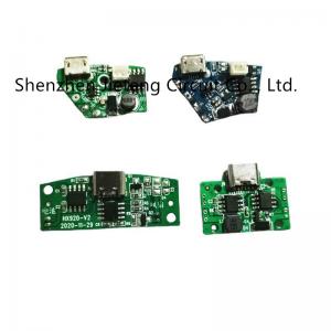
Manufacture PCB
Essential details
- Place of Origin:
Guangdong, China
- Base Material:
FR-4, glass epoxy, FR4 High Tg, Rohs compliant
- Copper Thickness:
1/2OZ 1OZ 2OZ 3OZ
- Board Thickness:
0.4~4.0mm
- Min. Hole Size:
0.01'',0.25mm.or 10 mil
- Min. Line Width:
0.006'' or 0.15mm
- Min. Line Spacing:
3mil
- Surface Finishing:
HASL, Immersion gold
- Number of layer:
1-60 layers
- Copper thickness tolerance:
± 0.25oz
- Solder mask:
Green, red, white, yellow, blue, black, etc
- Silk screen:
White, yellow, black, or negative
PCB Lead time (workday(s)) |
| Single, Double-sided | 4 layer | 6 layer | Over 8 layer | HDI |
Sample Lead time (Normal) | 4~5 days | 6~7 days | 7~8 days | 10~12 days | 10~12 days |
Sample Lead time (Faster) | 2~3 days | 3~5 days | 6 days | 6~7 days | 12 days |
Mass production lead time | 7~10 days | 10~14 days | 13-14 days | 16 days | 20 days |
Company Profile
Shenzhen Jieteng Circuit Co., Ltd. is a one-stop service company
integrating PCB circuit board prototyping, PCBA, and mass
production. The company has engineers with more than 10 years of
experience in this industry, providing customers with constructive
advice on circuit board production to avoid hidden dangers, provide
high-quality PCB circuit board production, and reduce the loss rate
of PCB circuit boards. PCBs procured by customers, as well as
complaint rates and procurement costs, shorten the customer's
procurement cycle. The company's main products include:
double-sided and multi-layer fiberglass PCB,
polytetrafluoroethylene PCB, polyimide flexible board FPC and
aluminum substrate PCB. Products are widely used in high-tech
education fields such as communications, power supply, computer
networks, digital products, industrial control, science and
education, lighting, aerospace, and national defense. Our customers
are all over the world, including the United Kingdom, Russia,
Brazil, Australia, South Korea, etc. We welcome friends from all
walks of life to visit, provide guidance and negotiate business.