
Add to Cart
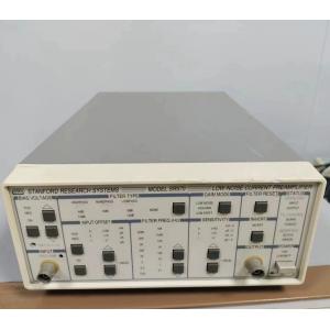
Tested In Full Working Condutions Stanford Research Systems SR570 Amplifiers
Description of Stanford Research Systems SR570 Amplifiers
The SR570 is a low-noise current preamplifier capable of current
gains as large as 1 pA/V. High gain and bandwidth, low noise, and
many convenient features make the SR570 ideal for a variety of
photonic, low temperature and other measurements.
Gain
The SR570 has sensitivity settings from 1 pA/V to 1 mA/V that can
be selected in a 1-2-5 sequence. A vernier gain adjustment is also
provided that lets you select any sensitivity in between.
Gain can be allocated to various stages of the amplifier to
optimize the instruments performance. The low noise mode places
gain in the front end of the amplifier for the best noise
performance. The high bandwidth mode allocates gain to the later
stages of the amplifier to improve the frequency response of the
front end. In the low drift mode, the input amplifier is replaced
with a very low input-current op amp, reducing the instrument’s DC
drift by up to a factor 1000.
Input Offset and DC Bias
An input offset-current adjustment is provided to suppress any undesired DC background currents. Offset currents can be specified from ±1 pA to ±1 mA in roughly 0.1 % increments. The SR570 also has an adjustable input DC bias voltage (±5 V) that allows you to directly sink current into a virtual null (analog ground) or a selected DC bias.
Toggle and Blanking
Two rear-panel, opto-isolated TTL inputs provide additional control
of the SR570. A blanking input lets you quickly turn off/on the
instrument's gain which is useful in preventing
Battery Operation
Three rechargeable lead-acid batteries provide up to 15 hours of
No Digital Noise
The microprocessor that runs the SR570 is "asleep" except during the brief interval it takes to change the instrument's setup. This ensures that no digital noise will contaminate low-level analog signals.
| SR570 Specifications | |||
| Input | |||
| Inputs | Virtual null or user-set bias (±5 V) | ||
| Input offset | ±1 pA to ±1 mA adjustable DC offset current | ||
| Maximum input | ±5 mA | ||
| Noise | See table below | ||
| Sensitivity | 1 pA/V to 1 mA/V in 1-2-5 sequence (vernier adj. in 0.5 % steps) | ||
| Frequency response | ±0.5 dB to 1 MHz. Adjustable front-panel frequency response compensation for source capacitance. | ||
| Grounding | Amplifier ground is fully floating. Amplifier and chassis ground are available at rear panel. Input ground can float up to ±40 V. | ||
| Filters | |||
| Signal filters | 2 configurable (low-pass or high-pass) 6 dB/oct rolloff filters. -3
dB points are settable in a | ||
| Gain allocation | |||
| Low noise | Gain is allocated to the front end for best noise performance. | ||
| High bandwidth | Front-end gain is reduced for optimum frequency response. | ||
| Low drift | Low bias current amplifier is used for reduced drift at high sensitivity. | ||
| Filter reset | Long time constant filters may be reset with front-panel button. | ||
| Output | |||
| Gain accuracy | ±0.5 % of output + 10 mV (25 °C) | ||
| DC drift | See table below | ||
| Maximum output | ±5 V into a high impedance load | ||
| General | |||
| External blanking | TTL input sets gain to zero | ||
| External toggle | TTL input inverts gain polarity | ||
| Rear panel biasing | ±12 VDC @ 200 mA, referenced to amplifier ground | ||
| Computer interface | RS-232, 9600 baud, receive only | ||
| Power | 100/120/220/240 VAC, 6 watts charged, 30 watts while charging. Internal batteries provide 15 hours of operation between charges. Batteries are charged while connected to the line. | ||
| Dimensions | 8.3" × 3.5" × 13.0" (WHL) | ||
| Weight | 15 lbs. (batteries installed) | ||
| Warranty | One year parts and labor on defects in materials and workmanship | ||
1.Can you ship order to Canada or Australia ?
Yes,we can .We send orders worldwide .
2. What delivery method do you use ? and delivery time ?
We can ship by EMS,DHL,FedEx,UPS,TNT with tracking number. Usual
delivery time is 4-7 workdays.
3. What is your payment term?
100% T/T payment before shipment.
4. How can I ask any other question ?
You can contact us online or leave us messages below .