Dual Layer Flexible Printed Circuit Board FPCB on Polyimide with Immersion Gold and Impedance control for USB Connector
Brand Name:Bicheng Enterprise Limited
Certification:UL
Model Number:BIC-0300-V3.0
Minimum Order Quantity:1 PIECE
Delivery Time:8-9 WORKING DAY
Payment Terms:T/T,Paypal
Contact Now
Add to Cart
Site Member
Location:
Shenzhen Guangdong China
Address:
6-11C Shidai Jingyuan Fuyong Town, Baoan District, Shenzhen City, Guangdong Province, China
Supplier`s last login times:
within 1 hours
Product Details
Company Profile
Product Details
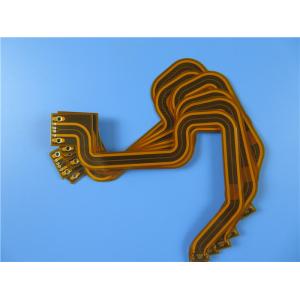
Dual Layer Flexible Printed Circuit Board FPCB on Polyimide with
Immersion Gold and Impedance control for USB Connector
(Flexible printed circuits are custom-made products, the picture
and parameters shown are just for reference)
General description
This is a type of flexible PCB built on polyimide 76 micron
substrate with 90 ohm impedance controlled on 0.15mm/0.3mm track
and gap for the application of USB Connector. It's standard 0.20 mm
thick with yellow solder mask (coverlay) on both sides and
immersion gold are on pads. FR-4 as stiffener is on the head and
tail. The base material is used from Shengyi, entire board
supplying 1 up flex per panel. They're fabricated per IPC 6012
Class 2 using supplied Gerber data. Each 25 pieces are packed for
shipment.
Parameter and data sheet
| PCB Size: | 116 X 108mm = 1 PCS |
| Number of Layers | 2 layers |
| Board Type | Flexbile PCB |
| Board Thickness | 0.2mm +/-10% |
| Stackup | TOP FR-4 Steffener 0.8mm |
| PI coverlay 0.025mm | |
| Copper top 0.035mm finish | |
| Polyimide substrate 0.076mm | |
| Copper top 0.035mm finish | |
| PI coverlay 0.025mm | |
| Board Material Supplier | Shengyi |
| Tg Value of Board Material | 60℃ |
| PTH Cu thickness | 20 um |
| Inner Iayer Cu thicknes | N/A |
| Surface Cu thickness | 35 um (1oz) |
| Coverlay Colour | Yellow |
| Number of Coverlay | 2 |
| Thickness of Coverlay | 25 um |
| Stiffener | FR-4 0.8mm |
| Type of Silkscreen Ink | N/A |
| Supplier of Silkscreen | N/A |
| Color of Silkscreen | N/A |
| Number of Silkscreen | N/A |
| Minimum via (mm) | 0.3 |
| Minimum Trace (mil) | 5.90 |
| Minimum Gap(mil) | 11.8 |
| Surface Finish | Immersion Gold |
| RoHS Required | Yes |
| Famability | 94-V0 |
| Thermal Shock Test | Pass, -25℃±125℃, 1000 cycles. |
| Thermal Stress | Pass, 300±5℃,10 seconds, 3 cycles. No delamination, no blistering. |
| Function | 100% Pass electrical test |
| Workmanship | Compliance with IPC-A-600H & IPC-6013C Class 2 |
| Type of artwork to be supplied | email file, Gerber RS-274-X, PCBDOC etc |
| Service area | Worldwide, Globally. |
Features and benefits
Excellent flexibility;
Reducing the volume;
Weight reduction;
Consistency of assembly;
Increased reliability;
Powerful PCB capabilities support your research and development,
sales and marketing;
Delivery on time with higher than 98% on-time-delivery rate;
Team with passion, discipline, responsibility and honesty;
No minimum order quantity. 1 piece is available;
Applications
Flexible flat cable, Industrial control temperature controller soft
board, medical equipment controller, automobile GPS navigation flex
board, tablet keypad flex board, display backlight
Structure of FPC
According to the number of layers of conductive copper foil, FPC
can be divided into single layer circuit, double layer circuit,
multi-layer circuit, double sided and so on.
Single-layer structure: the flexible circuit of this structure is the simplest structure
of the flexible PCB. Usually the base material (dielectric
substrates) + transparent rubber(adhesive) + copper foil is a set
of purchased raw materials(semi-manufactures), the protective film
and transparent glue are another kind of bought raw material.
First, copper foil must be etched to obtain the required circuit,
and the protective film should be drilled to reveal the
corresponding pad. After cleaning, the two are combined by rolling.
Then the exposed part of the pad electroplated gold or tin to
protect. In this way, the big panel board will be ready. Generally
also it’s stamped into the corresponding shape of the small circuit
board. There is also no protective film directly on the copper
foil, but printed resistance soldering coating, so that the cost
will be lower, but the mechanical strength of the circuit board
will become worse. Unless the strength requirement is not high and
the price needs to be as low as possible, it is best to apply the
protective film method.
Double layer structure: when the circuit is too complex to be wired, or copper foil is
needed to shield the ground, it is necessary to choose a double
layer or even a multilayer. The most typical difference between a
multilayer and a single plate is the addition of a perforated
structure to connect the layers of copper foil. The first process
of transparent rubber + base material + copper foil is to make
holes. Drill holes in the base material and copper foil first,
clean and then plated with a certain thickness of copper. The
subsequent fabrication process is almost the same as the
single-layer circuit.
Double sided structure: both sides of the double sided FPC have pads, mainly used to
connect other circuit boards. Although it and monolayer structure
is similar, but the manufacturing process is very different. Its
raw material is copper foil, protective film and transparent glue.
The protective film should be drilled according to the position of
the pad first, then the copper foil should be affixed, the pad and
track lines should be etched and then the protective film of
another drilled hole should be affixed.


Dual Layer Flexible Printed Circuit Board FPCB on Polyimide with Immersion Gold and Impedance control for USB Connector
Inquiry Cart
0