
Add to Cart
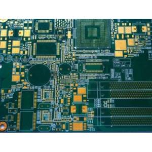
6-Layer HDI mobile phone PCB layout OSP Surface Finishing Board
Description
1. Professional manufacturer of PCB and PCB assembly specialized in single-sided PCB, double-sided PCB, multilayer PCB, PCB layout and design and PCB assembly
2. Material Type: FR4,non-halogen material ,Aluminium Base,Cooper Base,high frequency material ,Thick copper foil,94-V0(HB),PI Material,HIGH TG:SL S1000-2,ITEQ:IT180
3. Surface treatment: HAL,Immersion Gold,Immersion Tin,Immersion silver,Gold Finger,OSP,HAL(Immersion Gold,OSP,Immersion silver,Immersion Tin)+Gold Finger
PCB Capability
| High precision prototype | PCB bulk production | ||
| Max Layers | 1-28 layers | 1-14 layers | |
| MIN Line width(mil) | 3mil | 4mil | |
| MIN Line space(mil) | 3mil | 4mil | |
| Min via (mechanical drilling) | Board thickness≤1.2mm | 0.15mm | 0.2mm |
| Board thickness≤2.5mm | 0.2mm | 0.3mm | |
| Board thickness>2.5mm | Aspect Ration≤13:1 | Aspect Ration≤13:1 | |
| Aspect Ration | Aspect Ration≤13:1 | Aspect Ration≤13:1 | |
| Board thickness | MAX | 8mm | 7mm |
| MIN | 2 layers:0.2mm;4 layers:0.35mm;6 layers:0.55mm;8 layers:0.7mm;10 layers:0.9mm | 2 layers:0.2mm;4 layers:0.4mm;6 layers:0.6mm;8layers:0.8mm | |
| MAX Board size | 610*1200mm | 610*1200mm | |
| Max copper thickness | 0.5-6oz | 0.5-6oz | |
Immersion Gold/ Gold Plated Thickness | Immersion Gold:Au,1—8u” Gold finger:Au,1—150u” Gold Plated:Au,1—150u” Nickel Plated :50—500u” | ||
| Hole copper thick | 25um 1mil | 25um 1mil | |
| Tolerance | Board thickness | Board thickness≤1.0mm:+/-0.1mm 1.0mm<Board thickness≤2.0mm:+/-10% Board thickness>2.0mm:+/-8% | Board thickness≤1.0mm:+/-0.1mm 1.0mm<Board thickness≤2.0mm:+/-10% Board thickness>2.0mm:+/-8% |
| Outline Tolerance | ≤100mm:+/-0.1mm 100< ≤300mm:+/-0.15mm >300mm:+/-0.2mm | ≤100mm:+/-0.13mm 100< ≤300mm:+/-0.15mm >300mm:+/-0.2mm | |
| Impedance | ±10% | ±10% | |
| MIN Solder mask bridge | 0.08mm | 0.10mm | |
| Plugging Vias capability | 0.25mm--0.60mm | 0.70mm--1.00mm | |
How to get quick quotation?
| Step 1 Please send us Gerber file with these format: .CAD / .Gerber / .PCB / .DXP / .P-CAD, etc | ||||||||||||||||||||
| Step 2 Also please provide us the below details for quick quotation: | ||||||||||||||||||||
Board material: Fr - 4 / CEM - 1 / CEM - 3 / 22F / Fr - 1 / others | ||||||||||||||||||||
| Material brand: SY / KB / Rogers (optional) | ||||||||||||||||||||
| Material Specification:High Tg / copper based / aluminum based or others (optional) | ||||||||||||||||||||
| Board thickness: 0.1 - 6.0 mm | ||||||||||||||||||||
| Copper thickness: 0.05 Oz - 8 Oz ( 17 um - 288 um ) | ||||||||||||||||||||
| Surface Treatment: OSP / ENIG / HASL / Lead Free HASL / Immersion Tin / Immersion Sin | ||||||||||||||||||||
| Color of solder mask and silk print: Green / red / blue / black / white / yellow ,etc | ||||||||||||||||||||
| Board size and quantity | ||||||||||||||||||||
If you don't have Gerber file, please provide us the imfomation as step 2 or post your PCB Board to us for clone. | ||||||||||||||||||||
SAMPLE: | ||||||||||||||||||||
| ||||||||||||||||||||
| Layer count | Sample lead time/workday | Batch lead time/workday |
| 1-2L | 2 | 6 |
| 4L | 5 | 8 |
| 6L | 5 | 9 |
| 8L | 6 | 10 |
| 10L | 8 | 10 |
| 12L | 8 | 12 |
| 14L | 10 | 15 |
| 16L | 10 | 18 |
| 18-40L (Up to difficulty) | at least 18 | at least 24 |
| P.S. For HDI, Blind/Buried Hole PCB: Regular Lead Time + 3 workdays | ||
Q1: I am used to designing in metric units while the website is specified in imperial units.
A: When requesting an online quote, the quote form can handle mm units as well as inches for dimensions.
Q2: How do I specify internal cutouts/milling in my design?
A: All internal cutouts/slots/milling should be specified on the same layer is the board outline. The the minimum routable slot size is 32 mils. During order time, please state this requirement in the "Special Request" section so that our CAM engineers is aware of it. This is not something we encounter
Q3: What are the available holes sizes?
A: 14 mils to 150 mils - 1 mil increments 150 mils to 200 mils - 5 mil increments above 200 mils - holes would be routed out We only use drills in imperial units. Files submitted in metric units (mm) would be converted to imperial units (mils) and rounded up to the next mil.
Now send us your inquiry, and you will be replied within 8 hours!
Little knowledge - Metal Core PCB
Metal core PCB's are thermal management circuit boards which use a base metal material as the heat dissipater part of the PCB. They are used in high heat generating application like LED lighting in the area of high power LED lighting, Automotive Interior, Exterior Lighting, Parking Garage Lighting, LED spot light etc.
The metal core can be aluminum (aluminum core PCB) and copper (copper core PCB). The most common used aluminum core PCB is the thermal conductivity at 1W/MK and 2W/MK.

