
Add to Cart
Customized Piezo LiNbO3 LiTaO3 Wafer For Semiconductor POI And MEMS
Crystro can customize Surface Acoustic Piezoelectric Wafers including :
Lithium Niobate,Lithium Tantalate,Quartz Crystal as reuqired
cutting orientation and size,our Piezoelectric Effect crystals are
grown by Czochralski method. Max diameter reach 6inch,we can custom
size and specs ,rougness<0.5nm.
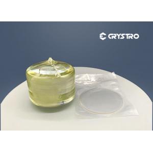
Dia 3" 4" 6" wafers are all available as per requirement.
Crystro possess Corning Flatmaster 200 Profiler, Laser marking
equipment, AOI and 6-step cleaning line.
Crystro provides:
Excellent photoelectric property
High Damage Threshold
High Curie Temperature
Basic Properties of LiTaO3:
| Material | Lithium Niobate | Lithium Tantalate | Quartz Crystal |
| Diameter / Size | 3’’, 4’’, 6’’, 8’’ | 3’’, 4’’, 6’’ | 3’’, 4’’, 5’’, 6’’, 8’’ |
| Cut Type | X / Y / Z | X / Y-Z / X-112Y | X / Y / Z |
| 36Y / 64Y/128Y | 28Y / 36Y / 42Y | AT / ST / DT | |
| Surface Finish | Double side polish / Single side polish | ||
| Thickness | 0.25mm / 0.35mm / 0.50mm / 1.00mm / 2.00mm | ||
| TTV | < 5um | ||
| PLTV | >98% (5mm*5mm) | ||
| LTV | < 1.5um | ||
| Bow | -25um < Bow < +25um | ||
| Warp | < 30um | ||
| Roughness | Ra<0.5nm, Ra<1nm | ||
| Curie Temp. | 1142℃ ± 2℃ | 605℃ ± 2℃ | 573℃ |
| Edge Profile | Round Ground, "C" Shape | ||
| Flats | 22±2mm, 32.5±2mm, 47.5±2mm, 57.5±2mm, Notch | ||
| As per request | |||
| Dope with | Er, MgO | Fe | with or without seed |
| Front Side | Roughness Ra<= 10A | ||
| Back Side | Roughness Ra: 0.2--0.7um GC#1000, GC#2000 | ||
| Appearance | No Cracks, saw marks, stains | ||
| Single Domian | Completed Polarization / Reduced | No Stress | |