Product Details
8inch Si Wafer Si Substrate 111 P Type N Type for
Micro-electromechanical systems (MEMS) Or Power semiconductor
devices Or Optical components and sensors
Product Description: The 8-inch silicon wafer with (111) crystal orientation is a
high-quality, single-crystal material widely used in semiconductor
manufacturing. The (111) crystal orientation provides specific
electrical and mechanical properties that are beneficial for
various high-performance applications.
Key Features:
- Diameter: 8 inches (200 mm).
- Crystal Orientation: (111), offering unique surface properties, ideal for certain
semiconductor processes and device characteristics.
- High Purity: Manufactured with a high level of purity to ensure uniformity and
low defect rates, critical for semiconductor and microelectronics
applications.
- Surface Quality: Typically polished or cleaned to meet stringent surface
requirements for device manufacturing.
Applications:
- Power Semiconductor Devices: The (111) orientation is preferred in certain power devices due to
its high breakdown voltage and favorable thermal properties.
- MEMS (Microelectromechanical Systems): Often used for sensors, actuators, and other micro-scale devices,
thanks to its well-defined crystal structure.
- Optoelectronic Devices: Suitable for applications in light-emitting devices and
photodetectors, where high crystal quality is important.
- Solar Cells: (111)-oriented silicon is also used in high-efficiency
photovoltaic cells, benefiting from enhanced light absorption and
carrier mobility.
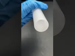
Application picture of Si Wafer:
Customizations:
- Thickness and Resistivity: These can be tailored according to customer specifications to meet
specific application requirements.
- Doping Type: P-type or N-type doping is available to adjust the wafer’s
electrical characteristics.
This silicon wafer type is crucial for a wide range of
semiconductor applications, providing a balance of mechanical
strength, electrical performance, and ease of processing.
Company Profile
SHANGHAI FAMOUS TRADE CO.,LTD. locates in the city of Shanghai,
Which is the best city of China, and our factory is founded in Wuxi
city in 2014.
We specialize in processing a varity of materials into wafers,
substrates and custiomized optical glass parts.components widely
used in electronics, optics, optoelectronics and many other fields.
We also have been working closely with many domestic and oversea
universities, research institutions and companies, provide
customized products and services for their R&D projects.
It's our vision to maintaining a good relationship of cooperation
with our all customers by our good reputatiaons.