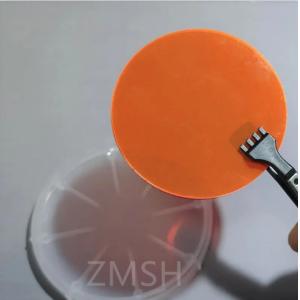
GaP wafer 2inch with OF Location/Length EJ 0-1-1 / 16±1mm LED LD
Mobility Min 100
Product Description:
A GaP wafer is a semiconductor substrate primarily used in the
fabrication of various electronic and optoelectronic devices.
Gallium Phosphide (GaP) wafers exhibit exceptional optical and
electronic properties that make them indispensable in the field of
semiconductor technology. These wafers are renowned for their
ability to generate light across different spectrums, allowing for
the production of LEDs and laser diodes in colors ranging from red,
green, to yellow.
The wide bandgap of approximately 2.26 electron volts (eV) enables
GaP wafers to efficiently absorb specific wavelengths of light.
This feature is crucial for optoelectronic applications, making GaP
an excellent choice for photodetectors, solar cells, and other
devices requiring tailored light absorption.
Furthermore, GaP demonstrates robust electronic conductivity and
thermal stability, making it suitable for high-frequency electronic
devices and applications where thermal management is essential.
GaP wafers not only serve as the base material for device
manufacturing but also function as substrates for the epitaxial
growth of other semiconductor materials. Their chemical stability
and relatively matched lattice parameters provide a favorable
environment for the deposition and fabrication of high-quality
semiconductor layers.
In essence, GaP wafers are highly versatile semiconductor
substrates, pivotal in the production of LEDs, laser diodes,
high-frequency electronic devices, and a spectrum of optoelectronic
components due to their superior optical, electronic, and thermal
properties.
Features:
- Product Name: Semiconductor Substrate GaP Wafer
- Ultra-thick silicon oxide wafer
- Silicon oxide wafer
- GaP Wafer Conduct Type: S-C-N
- Conductivity
- Mobility: Min 100
- GaP Wafer Orientation Angle: N/A
- GaP Wafer Particle Count: N/A
- Thickness: Min 175 Max 225
- Electrical Conductivity: GaP demonstrates good electrical
conductivity, contributing to its use in high-frequency electronic
devices and applications where reliable electronic performance is
essential.
- Thermal Stability: GaP exhibits notable thermal conductivity and
stability, making it suitable for applications requiring effective
thermal management.
- Substrate Functionality: GaP wafers serve not only as the
foundation material for device fabrication but also as substrates
for epitaxial growth, allowing the deposition of additional
semiconductor layers. Their compatibility with other materials and
relatively matched lattice parameters facilitate the growth of
high-quality semiconductor layers.
Technical Parameters:
| Parameter | Value |
|---|
| Orientation Angle | N/A |
| Surface Finish-back | Polished |
| Ingot CC | Min:1E17 Max:1E18 Cm³ |
| Grade | A |
| Epi-Ready | Yes |
| OF Location/Length | EJ[0-1-1]/ 16±1mm |
| Warp | Max:10 |
| Particle Count | N/A |
| Dopant | S |
| Resistivity | Min:0.01 Max:0.5 Ω.cm |
Applications:
- Manufacturing LEDs and Laser Devices: GaP wafers are used in the
fabrication of light-emitting diodes (LEDs) and laser diodes (LDs).
Their exceptional optical properties enable the production of light
in various wavelengths such as red, green, and yellow. This makes
GaP vital for applications in illumination, displays, indicator
lights, and laser devices.
- GaP Wafer Photodetectors: GaP is employed in the manufacturing of
photodetectors due to its superior light absorption capabilities at
specific wavelengths. These detectors are utilized for receiving
and detecting light signals within specific wavelength ranges,
including infrared light.
- GaP Wafer Solar Cells: GaP solar cells, while potentially having
lower efficiency compared to other materials, exhibit good light
absorption properties within certain spectra. This makes them
suitable for specific wavelength ranges in photovoltaic
applications.
- Semiconductor Devices: GaP, as a semiconductor material, is
utilized in the preparation of optical devices designed for
specific wavelength ranges. Additionally, owing to its electronic
characteristics, GaP is used in the manufacture of high-frequency
electronic devices.
- Overall, GaP wafers play a crucial role in the fields of
optoelectronics and semiconductor devices. They are especially
significant in applications involving LEDs, laser devices,
photodetectors, and optical devices designed for specific
wavelength ranges.
Customization:
ZMSH GaP Wafer Customized Service
Brand Name: ZMSH
Model Number: GaP Wafer
Place of Origin: China
BOW: Max:10
Material: GaP
IF Location/Length: EJ[0-1-1]/7±1mm
Grade: A
Dopant: S
We provide customized services for ZMSH GaP Wafer with thin film
technology and electro-oxidation, using high quality semiconductor
material.
Support and Services:
Semiconductor Substrate Technical Support and Service
We provide technical support and service for our Semiconductor
Substrate products. Our support and service include:
- 24/7 technical support hotline
- Free software and firmware updates
- On-site maintenance and repair services
- Online technical support forum
- Remote diagnosis and troubleshooting
- Replacement parts and accessories
Our team of experienced engineers is available to answer any
questions and provide help with installation, setup, and
troubleshooting. We believe in providing the highest level of
customer service. Contact us today to learn more about our
technical support and service.