
Add to Cart
2inch 3inch 4inch 5inch 6inch 8inch 12inch FZ CZ N-type polished silicon wafer DSP SiO2 wafers Silicon oxide wafer
1inch 2inch 10x10mm Scanning electron microscope silicon wafer small square piece SEM
Polished Silicon Wafer High-purity (11N) 1-12 inch single- and
double-polished Czochralski wafers
Sizes 1" 2" 3" 4" 5" 6" 8" 12" and special size and specification
wafers
Surface Single polishing disc, double polishing disc, abrasive
disc, corrosion disc, cutting disc
Crystal orientation <100> <111> <110> <211>
<511> and silicon wafers with various off-angles
Thickness 100um 200um 300um 400um 500um 1mm 5mm and other
thicknesses, thickness tolerance +-10um,
TTV< 10um or according to customer requirements, roughness
<0.2nm
Conductivity type N-type, P-type, undope (intrinsically high
resistance)
Single crystal method Czochralski (CZ), zone melting (FZ), NTD
(middle photo)
Resistivity Re-doping can reach <0.001 ohm.cm, low-doping
conventional 1~10 ohm.com, medium-light conventional 500~800
ohm.cm,
zone melting intrinsic: > 1000 ohm.cm, >3000 ohm.cm, >5000
ohm.cm, >8000 ohm.cm, >10000 ohm.cm
Process parameters Flatness TIR: ≤3μm, Warpage TTV: ≤10μm,
Bow/Warp≤40μm, roughness≤0.5nm, particle size <≤10ea@ > 0.3μ)
Packing method Ultra-clean aluminum foil vacuum packaging 10
pieces, 25 pieces
Processing customization The processing time of model, crystal
orientation, thickness, resistivity, etc. is slightly different
according to different specifications and parameters.
Application introduction It is used for synchrotron radiation
sample carriers such as processes, PVD/CVD coatings as substrates,
magnetron sputtering growth samples, XRD, SEM,
Atomic force, infrared spectroscopy, fluorescence spectroscopy and
other analysis test substrates, molecular beam epitaxy growth
substrates, X-ray analysis of crystalline semiconductors
ZMSH is Semiconductor strength factory, special for scientific research laboratory equipment testing, 2-3-4-5-6-8 inch polished silicon oxide wafers, high-purity single crystal silicon coated electron microscope scientific research substrate wafers
Please consult the owner before placing an order for specific specifications, and please feel free to ask any questions about silicon wafers.
All scientific research laboratories and semiconductor companies are welcome to order, and OEM orders can be received, and silicon wafers can be imported.
Special statement: All silicon wafers of our company are processed
from single crystal silicon drawn from native polysilicon, not
cheap recycled silicon wafers or used re-polished silicon wafers!
The quotation includes a 16% VAT invoice.
Our inventory list for Silicon Wafers (IC Grade, Pull Method CZ)
Straight Pull Single Side Polished Silicon Wafer
1 inch (25.4mm) single-sided polished Czochralski wafer thickness
500um
2 inches (50.8mm) single-sided polished Czochralski wafer thickness
280um
3 inches (76.2mm) single-sided polished Czochralski wafer thickness
380um
4-inch (100mm) single-sided polished straight-pull silicon wafer
with a thickness of 500um
5-inch (125mm) single-sided polished Czochralski wafer thickness
625um
6 inches (150mm) single-sided polished Czochralski wafer thickness
675um
Czochralski double-sided polished silicon wafers
1 inch (25.4mm) double-sided polished Czochralski wafer thickness
500um
2 inches (50.8mm) double-sided polished Czochralski wafer thickness
280um
3 inches (76.2mm) double-sided polished Czochralski wafer thickness
380um
4 inches (100mm) double-sided polished Czochralski wafer thickness
500um
5 inches (125mm) double-sided polished Czochralski wafer thickness
625um
6 inches (150mm) double-sided polished Czochralski wafer thickness
675um
Straight-pulled single-sided polished ultra-thin silicon wafers
1 inch (25.4mm) single-sided polished ultra-thin straight-pull
silicon wafer thickness 100um
2 inches (50.8mm) single-side polished ultra-thin straight-pull
silicon wafer thickness 100um
3 inches (76.2mm) single-side polished ultra-thin straight-pull
silicon wafer thickness 100um
4-inch (100mm) single-sided polished ultra-thin straight-pull
silicon wafer with a thickness of 100um
Czochralski double-sided polished ultra-thin silicon wafers
1 inch (25.4mm) double-sided polished ultra-thin Czochralski wafer
thickness 100um
2 inches (50.8mm) double-sided polished ultra-thin Czochralski
wafer thickness 100um
3 inches (76.2mm) double-sided polished ultra-thin Czochralski
wafer thickness 100um
4 inches (100mm) double-sided polished ultra-thin Czochralski wafer
thickness 100um
Silicon wafer (IC grade, zone melting FZ)
Zone melting single-side polished silicon wafer
1-inch (25.4mm) fused silicon wafer thickness 500um in single-sided
polishing area
2 inches (50.8mm) fused silicon wafer thickness 280um in
single-side polishing area
3-inch (76.2mm) fused silicon wafer thickness 380um in single-side
polishing area
4 inches (100mm) fused silicon wafer thickness 500um in single-side
polishing area
Zone melting double-sided polished silicon wafers
1 inch (25.4mm) fused silicon wafer thickness 500um in double-sided
polishing area
2 inches (50.8mm) fused silicon wafer thickness 280um in
double-sided polishing area
3-inch (76.2mm) fused silicon wafer thickness 380um in double-sided
polishing area
4 inches (100mm) fused silicon wafer thickness 500um in
double-sided polishing area
Zone melting single-side polished ultra-thin silicon wafer
1-inch (25.4mm) single-sided polishing zone melting ultra-thin
silicon wafer thickness 100um
2 inches (50.8mm) single-sided polishing zone melting ultra-thin
silicon wafer thickness 100um
3 inches (76.2mm) single-sided polishing zone melting ultra-thin
silicon wafer thickness 100um
4 inches (100mm) single-sided polishing zone melting ultra-thin
silicon wafer thickness 100um
Zone melting double-sided polished ultra-thin silicon wafers
1 inch (25.4mm) double-sided polishing area melting ultra-thin
silicon wafer thickness 100um
2 inches (50.8mm) double-sided polishing area melting ultra-thin
silicon wafer thickness 100um
3 inches (76.2mm) double-sided polishing area melting ultra-thin
silicon wafer thickness 100um
4 inches (100mm) double-sided polishing area melting ultra-thin
silicon wafer thickness 100um
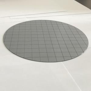
Product parameters. for 8inch si wafers
Product Size. 8-inch single-sided polished silicon wafer
production methods. Czochralski (CZ)
Diameter and tolerance mm. 200±0.3mm
Model/Doping Type. N type (phosphorus, arsenic) P type (boron
doped)
crystal orientation. <111><100><110>
Resistivity. 0.001-50 (ohm-cm) (different resistivity ranges can be
customized according to customer requirements)
Flatness TIR. <3um; Warpage TTV. <10um; Bending BOW. <10um
Roughness Ra <0.5nm; Granularity pewaferr <10@0.3um
Packing 25 pieces package 100-level clean room double-layer vacuum
packaging
Used for synchrotron radiation sample carriers such as processes,
PVD/CVD coating as substrate, magnetron sputtering growth samples,
XRD, SEM, atomic force, infrared spectroscopy, fluorescence
spectroscopy and other analysis and testing substrates, molecular
beam epitaxy growth substrates, X-ray analysis Crystal
Semiconductor Lithography
Ordering information must include:
1. Resistivity
2. Size: 2", 3", 4", 5", other sizes can be customized
3. Thickness
4. One-sided polishing, double-sided polishing, no polishing
5. Grade: Mechanical Grade, Test Grade, Prime Grade (Positive Film)
6. Conductivity type: P type, N type
7. Crystal orientation
7. Doping type: boron-doped, phosphorus-doped, arsenic-doped,
gallium-doped, antimony-doped, undoped
8. TTV, BOW (normal value is <10um)

