Product Details
2inch 4iinch 6Inch Sapphire based AlN templates AlN film on
sapphire substrate
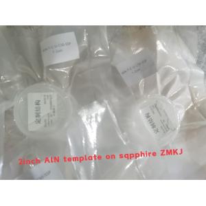
2inch on sapphire substrate AlN Template layer Wafer For 5G BAW
Devices
Applications of AlN template
Our OEM has developed a serials of proprietary technologies and
the-state-of-the art PVT growth reactors and facilities to
fabricate different sizes of high-quality single crystalline AlN
wafers, AlN temlpates. We are one of the few world-leading
high-tech companies who own full AlN fabrication capabilities to
produce high-quality AlN boules and wafers, and provide
professional services and turn-key solutions to our
customers,arranged from the growth reactor and hotzone design,
modeling and simulation, process design and optimization, crystal
growth,
wafering and material characterization. Up to April 2019, they have
applied more than 27 patents (including PCT).
Specification
Characteristic Specification
Other relaterd 4INCH GaN Template Specification
| GaN/ Al₂O₃ Substrates (4") 4inch |
| Item | Un-doped | N-type | High-doped N-type |
| Size (mm) | Φ100.0±0.5 (4") |
| Substrate Structure | GaN on Sapphire(0001) |
| SurfaceFinished | (Standard: SSP Option: DSP) |
| Thickness (μm) | 4.5±0.5; 20±2;Customized |
| Conduction Type | Un-doped | N-type | High-doped N-type |
| Resistivity (Ω·cm)(300K) | ≤0.5 | ≤0.05 | ≤0.01 |
GaN Thickness Uniformity
| ≤±10% (4") |
Dislocation Density (cm-2)
| ≤5×10⁸ |
| Useable Surface Area | >90% |
| Package | Packaged in a class 100 clean room environment. |
| Crystal structure | Wurtzite |
| Lattice constant (Å) | a=3.112, c=4.982 |
| Conduction band type | Direct bandgap |
| Density (g/cm3) | 3.23 |
| Surface microhardness (Knoop test) | 800 |
| Melting point (℃) | 2750 (10-100 bar in N2) |
| Thermal conductivity (W/m·K) | 320 |
| Band gap energy (eV) | 6.28 |
| Electron mobility (V·s/cm2) | 1100 |
| Electric breakdown field (MV/cm) | 11.7 |
Company Profile
SHANGHAI FAMOUS TRADE CO.,LTD. locates in the city of Shanghai,
Which is the best city of China, and our factory is founded in Wuxi
city in 2014.
We specialize in processing a varity of materials into wafers,
substrates and custiomized optical glass parts.components widely
used in electronics, optics, optoelectronics and many other fields.
We also have been working closely with many domestic and oversea
universities, research institutions and companies, provide
customized products and services for their R&D projects.
It's our vision to maintaining a good relationship of cooperation
with our all customers by our good reputatiaons.