5um Thickness AlN Aluminum Nitride Template 430um Sapphire 350um Sic Substrates
Brand Name:zmkj
Model Number:2-4inch template
Minimum Order Quantity:5pcs
Delivery Time:1-5weeks
Payment Terms:T/T, Western Union
Place of Origin:CHINA
Contact Now
Add to Cart
Verified Supplier
Location:
Shanghai Shanghai China
Address:
Rm5-616,NO.851,Dianshanhu road; Qingpu area;shanghai city//201799
Supplier`s last login times:
within 38 hours
Shipping
lt's easy to get a shipping quote! Just click the button below and complete the short form.
Get Shipping Quote
Product Details
Company Profile
Product Details
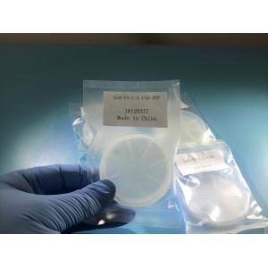
2inch 5um thickness AlN Aluminum Nitride Template on 430um sapphire/ 350um Sic substrates
AlN Wafer Characteristic
- III-Nitride(GaN,AlN,InN)
2inch AlN template on sapphire or sic substrates, HVPE Gallium Nitride wafer,AlN substrates on GaN
We offer single crystalline AlN substrates on c-plane sapphire
template,which called AlN wafer or AlN template,for UV LEDs,
semiconductor devices and AlGaN epitaxial growth.Our epi-ready,
C-plane AlN substrates have good XRD FWHM or dislocation density.
The available thickness is from 30nm to 5um.
Our single crystal Aluminum Nitride substrates with low dislocation
has widely application:including UV LED,detectors, IR seekers
windows, epitaxial growth of III-nitrides,Laser, RF transistors and
other semiconductor device.
Forbidden band width (light emitting and absorption) cover the
ultraviolet, visible light and infrared.
AlN template is used for development of HEMT structures, resonant
tunneling diodes and
acoustoelectronic devices
2-4 inch AlN templates Specification
Specifications:
| 2” AlN Templates | 4inch | |
| Item | AlN-T | |
| Dimensions | Ф 2” | |
| Substrate | Sapphire, SiC, GaN | |
| Thickness | 4-5um | |
| Orientation | C-axis(0001) ± 1° | |
| Conduction Type | Semi-Insulating | |
| Dislocation Density | XRD FWHM of (0002) < 200 arcsec. | |
| XRD FWHM of (10-12) < 1000 arcsec | ||
| Useable Surface Area | > 80% | |
| Polishing | Standard: SSP | |
| Option: DSP | ||
| Package | Packaged in a class 100 clean room environment, in cassettes of 25pcs or single wafer containers, under a nitrogen atmosphere. | |
Application:
GaN can be used in many areas such as LED display, High-energy
Detection and Imaging,
Laser Projection Display, Power Device, etc.
- High- Frequency Microwave Devices High-energy Detection and imagine
- New energy solor hydrogen technology Environment Detection and biological medicine
- Light source terahertz band
- Laser Projection Display, Power Device, etc. Date storage
- Energy-efficient lighting Full color fla display
- Laser Projecttions High- Efficiency Electronic devices
OUR RELATED PRODUCTS
Our Factroy Enterprise Vision
we will provide high quality GaN substrate and application
technology for the industry with our factory.
High quality GaNmaterial is the restraining factor for the
III-nitrides application, e.g. long life
and high stability LDs, high power and high reliability micro-wave
devices, High brightness
and high efficiency, energy-saving LED.
-FAQ –
Q: What's the MOQ?
(1) For inventory, the MOQ is 2pcs.
(2) For customized products, the MOQ is 5pcs-10pcs.
It depends on quantity and technics.
Q: Do you have inspection report for material?
We can supply ROHS report and reach reports for our products.
Q: What you can supply logistics and cost?
(1) We accept DHL, Fedex, TNT, UPS, EMS, SF and etc.
(2) If you have your own express number, it's great.
If not, we could assist you to deliver. Freight=USD25.0(the first
weight) + USD12.0/kg
Q: What's the delivery time?
(1) For the standard products such as 2inch 0.33mm wafer.
For inventory: the delivery is 5 workdays after order.
For customized products: the delivery is 2 or 4 workweeks after
order.
Q: How to pay?
100%T/T, Paypal, West Union, MoneyGram, Secure payment and Trade
Assurance.

5um Thickness AlN Aluminum Nitride Template 430um Sapphire 350um Sic Substrates
Inquiry Cart
0