
Add to Cart
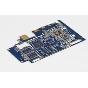
8 layers of order two HDI, FR-4, TG180,pcb prototype
assembly,rapid prototyping pcb,pcb assembly prototype,prototype
pcb,,prototype pcb service,prototype pcb,pcb rapid prototyping
Product Description
PCB, FPC product application field
Various digital products, automotive new energy, automotive
products, military, aerospace, medical, wireless terminals, wired
terminals, communication equipment, communication stations,
finance, industrial industrial control, consumer electronics,
educational equipment, smart devices, smart products, security,
LED, computer, mobile phone and other electronic products
Surface treatment: full board OSP, full board immersion gold, whole board electric
nickel gold, electric gold + immersion gold, electric gold + OSP,
OSP + immersion gold, OSP + carbon bridge, gold finger, OSP + gold
finger, immersion gold + gold finger, Shen tin, immersion silver,
lead-free tin spray
PCB, FPC process production capability
| Type | Jiangxi Chaosheng | Zhejiang Kunyu |
| Scope | Double Side,Multilayers(4-20) | Multilayers(4-28),HDI(4-20)Flex,Rigid Flex |
| Double Side | CEM-3, FR-4,Rogers RO4233,Bergquist Thermal Clad 12mil–126mil (0.3mm-3.2mm) | CEM-3, FR-4,Rogers RO4233,Bergquist Thermal Clad 4mil–126mil (0.1mm-3.2mm) |
| Multilayers | 4-20 layers, board thickness 15mil-126mil (0.38mm-3.2mm) | 4-28 layers, board thickness 8mil-126mil (0.2mm-3.2mm) |
| Buried/Blind Via | 4-18 layers, board thickness 15mil-126mil(0.38mm-3.2mm) | 4-20 layers, board thickness 10mil-126mil(0.25mm-3.2mm) |
| HDI | / | 1+N+1,2+N+2,3+N+3,Anylayer |
| Flex & Rigid-Flex PCB | / | 1-8layers Flex PCB ,2-12layers Rigid-flex PCB HDI+Rigid-flex PCB |
| Laminate | Shengyi,EMC,ITEQ,Panasionic,Hitachi.... | |
| Soldermask Type(LPI) | Taiyo,Goo’s,Probimer..... | Taiyo,Goo’s,Probimer FPC..... |
| Peelable Soldermask | Peters | |
| Carbon ink | Nipon | |
| HASL/Lead Free HASL | Thickness: 0.5-40um | Thickness: 0.5-40um |
| OSP | Entek Plus HT, Preflux F2 LX | |
| ENIG (Ni-Au) | Au:0.03um≤max<0.06um Ni:3um≤max≤6um | |
| Electro-bondable Ni-Au | Au:0.2-1.0um Ni:2.54-10um | |
| Electro-nickel palladium Ni-Au | Au: 0.015-0.075um Pd 0.02-0.075um Ni:2-6umm | |
| Electro. Hard Gold | Au:5~50uin(0.125~1.27um); Nithickness:100~250uin(2.50~6.25um) | |
| Thick tin | 1.0-1.4um | |
| Capability | Mass Production | Mass Production |
| Min Mechanical Drill Hole | 0.20mm | 0.20mm |
| Min. Laser Drill Hole | / | 4mil (0.100mm) |
| Line Width/Spacing | 3mil/3mil | 2mil/2mil |
| Max. Panel Size | 18.5" X 24.5"(470mm X 622mm) | 21.5" X 24.5"(546mm X 622mm) |
| Line Width/Spacing Tolerance | +/-10% ~ +/-20% | Non electro coating:+/-5um,Electro coating:+/-10um |
| PTH Hole Tolerance | +/-0.003inch(0.075mm) | +/-0.002inch(0.050mm) |
| NPTH Hole Tolerance | +/-0.002inch(0.050mm) | +/-0.002inch(0.050mm) |
| Hole Location Tolerance | +/-0.003inch(0.075mm) | +/-0.002inch(0.050mm) |
| Hole to Edge Tolerance | +/-0.004inch(0.100mm) | +/-0.004inch(0.100mm) |
| Edge to Edge Tolerance | +/-0.004inch(0.100mm) | +/-0.004inch(0.100mm) |
| Layer to Layer Tolerance | +/-0.004inch(0.100mm) | +/-0.003inch(0.075mm) |
| Impedance Tolerance | +/- 10% | +/- 10% |
| Warpage % | Max ≤0.75% | Max≤0.5% |
Technology (HDI Product)
| ITEM | Production | Tighten Control | |
| Laser Via Drill/Pad | 0.125/0.30 , 0.125/0.38 | 0.125/0.28 , 0.125/0.36 , 0.20/0.40 | |
| Blind Via Drill/Pad | 0.25/0.50 | 0.20/0.45 | |
| Line Width/Spacing | 0.10/0.10 | 0.075/0.075 | |
| Hole Formation | CO2 Laser Direct Drill | ||
| Build Up Material | FR4 LDP(LDD); RCC 50 ~100 micron | ||
| Cu Thickness on Hole Wall | Blind Hole: 10um(min) | Buried Hole: 13um(min) | |
| Aspect Ratio | 0.8 : 1 | ||
Technology (Flexible PCB)
| Project | Ability |
| Roll to roll (one side) | YES |
| Roll to roll (double) | NO |
| Volume to roll material width mm | 250 |
| Minimum production size mm | 250x250 |
| Maximum production size mm | 500x500 |
| SMT Assembly patch (Yes/No) | YES |
| Air Gap capability (Yes/No) | YES |
| Production of hard and soft binding plate(Yes/No) | YES |
| Max layers(Hard) | 10 |
| Tallest layer(Soft plate) | 6 |
| Material Science | |
| PI | YES |
| PET | YES |
| Electrolytic copper | YES |
| Rolled Anneal Copper Foil | YES |
| PI | |
| Covering film alignment tolerance mm | ±0.1 |
| Minimum covering film mm | 0.175 |
| Reinforcement | |
| PI | YES |
| FR-4 | YES |
| SUS | YES |
| EMI SHIELDING | |
| Silver Ink | YES |
| Silver Film | YES |
FAQ:
Q: What files do you use in PCB fabrication?
A: Gerber or Eagle, BOM listing, X, Y sitting report, PNP and
Components Position
Q: Is it possible you could offer sample?
A: Yes, we can custom you sample to test before mass production
Q: When will I get the quotation after sent Gerber, BOM and test
procedure?
A: Within 6-48hours for PCB quotation and around 24-48 hours for
PCBA quotation.
Q: According to the difficulty of high-layer boards, How can I know
the process of my PCB production?
A: 7-35days for PCB production and components purchasing, and
14-20days for PCB assembly and Testing
Q: How can I make sure the quality of my PCB?
A: We ensure that each piece of PCB, PCBA products work well before
shipping. We'll test all of them according to your test procedure.


