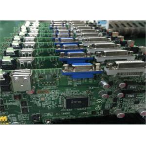
Copper PCB Heavy Copper PCB Hard Gold Metal Core 4 oz copper pcb
Brand Name:FOUND
Certification:UL E361831
Model Number:FD-56
Minimum Order Quantity:1
Payment Terms:T/T
Place of Origin:CHINA
Contact Now
Add to Cart
Active Member
Location:
Shenzhen Guangdong China
Address:
NO.1 Industry Park, XinSheng Village, Longgang District, ShenZhen
Supplier`s last login times:
within 1 hours
Shipping
lt's easy to get a shipping quote! Just click the button below and complete the short form.
Get Shipping Quote
Product Details
Company Profile
Product Details
Copper PCB Heavy Copper PCB Hard Gold Metal Core 4 oz copper pcb
General description
This is a type of 4 Layer Rogers PCB built on 0.508 mm (20 mil)
RO4350B with Tg 280°C for the
application of GPS tracker. Multilayer PCB's on Rogers material
have different structure (stack up)
from FR-4 multilayer PCB's, because the core of Rogers material is
semi-manufactures. For this 4
layer high frequency PCB, it uses 2 cores of 20mil RO4350B. Usually
blind via from layer 1 to layer
3 is hard to be drilled. On the other hand, the back drill
technology can solve this problem of signal
integrity.
Basic specifications
Base material: RO4350B 20 mil + RO4450B 4 mil
Layer count: 4 layers
Type: Mixed multiplier milled separately
Format: 70mm x 125mm = 1 piece
Surface finish: Immersion gold
Copper weight: Outer layer 35 um/ Inner layer 18 um
Solder mask / Legend: Green / white
Final PCB height: 1.42 mm
Standard: IPC 6012 Class 2
Packing: Each 25 panels are packed for shipment.
Lead time: 12 working days
Shelf life: 6 months
Features and benefits
Excellent high frequency performance due to low dielectric
tolerance and loss;
Low thermal coefficient of dielectric constant;
Stable electrical properties verus frequency;
Back drilling reducing noise interference;
ISO9001, ISO14001, UL certified manufacturing factory;
Strict WIP inspection and monitoring as well as working
instruction;
30000 square meter month capability;
8000 types of PCBs per month;
Product capability
| Material | FR-4 / Hi Tg FR-4 / Lead free Materials (RoHS Compliant) /CEM-1, Aluminium, Metal based | |
| Layer No. | 1-18 | |
| Finished Board thickness | 0.2 mm-3.8mm'(8 mil-150 mil) | |
| Board Thickness Tolerance | ±10% | |
| Cooper thickness | 0.5 OZ-6OZ (18 um-210um) | |
| Copper Plating Hole | 18-40 um | |
| Impedance Control | ±10% | |
| Warp&Twist | 0.70% | |
| Peelable | 0.012"(0.3mm)-0.02'(0.5mm) | |
| Images | ||
| Min Trace Width (a) | 0.075mm (3mil) | |
| Min Space Width (b) | 0.1mm (4 mil) | |
| Min Annular Ring | 0.1mm (4 mil) | |
| SMD Pitch (a) | 0.2 mm(8 mil) | |
| BGA Pitch (b) | 0.2 mm (8 mil) | |
| 0.05mm | ||
| Solder Mask | ||
| Min Solder Mask Dam (a) | 0.0635 mm (2.5mil) | |
| Soldermask Clearance (b) | 0.1mm (4 mil) | |
| Min SMT Pad spacing (c) | 0.1mm (4 mil) | |
| Solder Mask Thickness | 0.0007"(0.018mm) | |
| Holes | ||
| Min Hole size (CNC) | 0.2 mm (8 mil) | |
| Min Punch Hole Size | 0.9 mm (35 mil) | |
| Hole Size Tol (+/-) | PTH:±0.075mm;NPTH: ±0.05mm | |
| Hole Position Tol | ±0.075mm | |
| Plating | ||
| HASL | 2.5um | |
| Lead free HASL | 2.5um | |
| Immersion Gold | Nickel 3-7um Au:1-5u'' | |
| OSP | 0.2-0.5um | |
| Outline | ||
| Panel Outline Tol (+/-) | CNC: ±0.125mm, Punching: ±0.15mm | |
| Beveling | 30°45° | |
| Gold Finger angle | 15° 30° 45° 60° | |
| Certificate | ROHS, ISO9001:2008, SGS, UL certificate,CQC certificate | |
Advantages:
No MOQ
18 years of PCB&PCBA turnkey services
Quick turn, Prototype, Low & medium & high volume
Components sourcing,ODM&OEM services provide
ISO 9001-, ISO14001-, ISO/TS16949, ISO13485, IATF16949,
OHSAS18001certified,UL E361831
100% E-test,100% visual inspection, including IQC, IPQC, FQC and
OQC
100% AOI inspection, including X-ray, 3D microscope and ICT
Fast response within 24 hours,great pre-sales, sales, after-sales
Guarantee Sales Service,for all problems encountered kindly contact
us, we will do the after service any time.


Copper PCB Heavy Copper PCB Hard Gold Metal Core 4 oz copper pcb
Inquiry Cart
0