30L FR4 SMT PCB Assembly 7.0mm Thickness Lead Free HASL 94v0 Standard

Brand Name:KAZ
Certification:UL&ROHS
Model Number:KAZA-100
Minimum Order Quantity:1 Unit
Delivery Time:3-14 days
Payment Terms:T/T, Western Union, MoneyGram, L/C, D/A
Contact Now

Add to Cart

Verified Supplier
Location: Shenzhen Guangdong China
Address: Room 502, 26# Building, Funing Hi-Tech Industrial Park, Fuhai Street, Bao'an, Shenzhen, Guangdong, China, 518103
Supplier`s last login times: within 1 hours
Product Details Company Profile
Product Details

Ultrafast PCB fabrication manufacturer, offering one-stop PCB manufacturing, PCB assembly, SMT stencil,cheap and good quality pcb smt assembly


1. Features


1. One Stop OEM Service, PCB manufacturing Made in Shenzhen of China

2. Manufactured by Gerber File and BOM List from Customer

3. FR4 Material, Meet 94V0 standard

4. SMT, DIP technology suport

5. Lead Free HASL, Environmental Protection

6. UL, CE, ROHS Compliant

7. Shipping By DHL,UPS, TNT, EMS or Customer requirement


2. PCB Technical capability


SMTPosition accuracy:20 um
Components size:0.4×0.2mm(01005) —130×79mm,Flip-CHIP,QFP,BGA,POP
Max. component height::25mm
Max. PCB size:680×500mm
Min. PCB size:no limited
PCB thickness:0.3 to 6mm
PCB weight:3KG
Wave-SolderMax. PCB width:450mm
Min. PCB width: no limited
Component height:Top 120mm/Bot 15mm
Sweat-SolderMetal type :part, whole, inlay, sidestep
Metal material:Copper , Aluminum
Surface Finish:plating Au, plating sliver , plating Sn
Air bladder rate:less than20%
Press-fitPress range:0-50KN
Max. PCB size:800X600mm
TestingICT,Probe flying,burn-in,function test,temperature cycling

3.PCB Manufacturing Process


  1. 1.1 Step 1 – The Design.
  2. 1.2 Step 2 – Printing the Design.
  3. 1.3 Step 3 – Creating the Substrate.
  4. 1.4 Step 4 – Printing the Inner Layers.
  5. 1.5 Step 5 – Ultraviolet Light.
  6. 1.6 Step 6 – Removing Unwanted Copper.
  7. 1.7 Step 7 – Inspection.
  8. 1.8 Step 8 – Laminating the Layers.

4.The PCB Fabrication Process
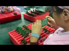

  • Imaging desired layout on copper clad laminates
  • Etching or removing excess copper from inner layers to reveal traces and pads
  • Creating the PCB layer stackup by laminating (heating and pressing) board materials at high temperatures
  • Drilling holes for mounting holes, through hole pins and vias
  • Etching or removing excess copper from the surface layer(s) to reveal traces and pads
  • Plating pin holes and via holes
  • Adding protective coating to surface or solder masking
  • Silkscreen printing reference and polarity indicators, logos or other markings on the surface
  • Optionally, a finish may be added to copper areas of surface

5.PCB Pictures


China 30L FR4 SMT PCB Assembly 7.0mm Thickness Lead Free HASL 94v0 Standard supplier

30L FR4 SMT PCB Assembly 7.0mm Thickness Lead Free HASL 94v0 Standard

Inquiry Cart 0