Add to Cart
1oz Copper Thickness White Soldmask HASL Surface PCB Printed Circuit Board PCB Assembly Service
How to place an order:
Manufacturing Capacity - Rigid PCB:
| Item | Production Capacity |
| Type of Products | Single Sided, double sided & multilayer |
| Max Board Size | Single & Double Sided: 600*1500mm |
| Multilayer: 600*1,200 mm | |
| Surface Finish | HASL, ENIG, OSP, Immersion Silver, Golden Finger, etc. |
| Layers | 1~20 |
| Boad Thickness | 0.4~4.0mm |
| Base Copper | 18um(1/2oz), 35um (1oz), 70um (2oz), 105um (3oz), 150um (4oz), 300um (8oz) |
| Board Material | FR-4, Aluminum base, Polymide, copper base, ceramic base |
| Min Drilling Hole Size | 0.1mm |
| Min Line Width & Space | 0.075mm |
| Platting Gold | Nickle Plating Thickness 2.5~5um, gold thickness 0.05~0.1um |
| Tin Spraying | Tin thickness 2.5~5um |
| Milling Space | wire & edge: 0.15mm, hole & edge: 0.2mm, Contour Tolerance: +/-0.1mm |
| Socket Chamfer | Angle: 30°/45°/60° Depth: 1~3mm |
| V-Cut | Angle: 30°/45°/60° Depth: 1/3 of board thickness, min aise: 80*80mm |
| On-Off Test | Max Testing Area: 400*1,200mm |
| Max Testing Point: 12,000 points | |
| Max Testing Voltage: 300V | |
| Max Insulation Resistance: 100mΩ | |
| Impedance Control Tolerance | ± 10% |
| Soldering Endurance | 85℃~105℃ / 280℃~360℃ |
Printed circuit boards (PCBs)are the basic components of electronic equipment and are the physical foundation that connects and supports various electronic components. It plays a vital role in the functionality and reliability of electronic systems.
Key aspects of electronic printed circuit boards include:
Layers and composition:
PCBs are typically made up of multiple layers, with the most common being a 2- or 4-layer design.
These layers are made of copper serving as conductive paths and a non-conductive substrate such as fiberglass (FR-4) or other specialty materials.
Other layers may include power and ground planes for power distribution and noise reduction.
Interconnects and Traces:
The copper layer is etched to form conductive traces that serve as pathways for electrical signals and power.
Vias are plated-through holes that connect traces between different layers, enabling multi-layer interconnections.
Trace width, spacing, and routing patterns are designed to optimize signal integrity, impedance, and overall electrical performance.
Electronic component:
Electronic components, such as integrated circuits, resistors, capacitors, and connectors, are mounted and soldered to the PCB.
The placement and routing of these components is critical to ensuring optimal performance, cooling, and overall system functionality.
PCB manufacturing technology:
PCB manufacturing processes typically involve steps such as lamination, drilling, copper plating, etching and solder mask application.
Advanced technologies such as laser drilling, advanced plating, and multi-layer co-lamination are used in specialized PCB designs.
PCB Assembly & Soldering:
Electronic components are placed and soldered onto the PCB either manually or automatically using techniques such as through-hole soldering or surface mount soldering.
Reflow soldering and wave soldering are common automated processes for connecting components.
Testing & Quality Control:
The PCB undergoes various testing and inspection processes such as visual inspection, electrical testing, and functional testing to ensure its reliability and performance.
Quality control measures, such as in-process inspections and design-for-manufacturability (DFM) practices, help maintain high standards in PCB production.
Electronic PCBs are used in a wide variety of applications, including consumer electronics, industrial equipment, automotive systems, medical devices, aerospace and telecommunications equipment, and more. Continuing advances in PCB technology, such as the development of high-density interconnect (HDI) PCBs and flexible PCBs, have enabled the creation of smaller, more powerful, and more energy-efficient electronic devices.
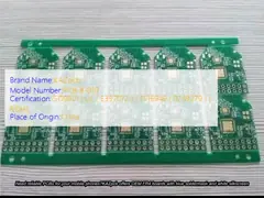
More photoes for this Double sided PCB with 1.6mm 1oz copper thickness HASL surface treatment white soldmask
Product Applicances
Product Show - Rigid PCB
Product Show - FPC
Product Show - PCB Assemblies