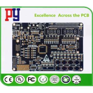
Black 2L Inverter 6oz 4mil PCB Printed Circuit Board HASL Lead Free
Brand Name:PY
Certification:ISO9001
Model Number:PCB
Minimum Order Quantity:1PCS
Delivery Time:5-10 work days
Payment Terms:T/T, L/C, D/A, D/P, Western Union, MoneyGram
Contact Now
Add to Cart
Verified Supplier
Location:
Shenzhen Guangdong China
Address:
West of 2nd Floor, Building 10, Zhengzhong Science Park, Xintian Community, Fuhai Street, Bao'an District, Shenzhen China 518103
Supplier`s last login times:
within 1 hours
Product Details
Company Profile
Product Details
Black 2L Inverter 6oz 4mil PCB Printed Circuit Board HASL Lead Free
| High precision prototype | PCB bulk production | ||
| Max Layers | 6 layers | 6 layers | |
| MIN Line width(mil) | 2mil | 4mil | |
| MIN Line space(mil) | 2mil | 4mil | |
| Min via (mechanical drilling) | Board thickness≤1.2mm | 0.2mm | 0.3mm |
| Board thickness≤2.5mm | 0.2mm | 0.3mm | |
| Board thickness>2.5mm | Aspect Ration≤13:1 | Aspect Ration≤13:1 | |
| Aspect Ration | |||
| Board thickness | MAX | 6mm | 6mm |
| MIN | 4 layers:0.35mm;6 layers:0.55mm; | 4 layers:0.4mm;6 layers:0.6mm; | |
| MAX Board size | 550*1100mm | 620*100mm | |
| Max copper thickness | 6oz | 6oz | |
| Immersion Gold/ Gold Plated Thickness | Immersion Gold:Au,1—8u” Gold finger:Au,1—150u” | ||
| Hole copper thick | 25um 1mil | 25um 1mil | |
| Tolerance | Board thickness | thickness≤2.0mm:+/-10% Board thickness>2.0mm:+/-8% | thickness≤2.0mm:+/-10% Board thickness>2.0mm:+/-8% |
| Outline Tolerance | ≤100mm:+/-0.1mm 100< ≤300mm:+/-0.15mm | ≤100mm:+/-0.13mm 100< ≤300mm:+/-0.15mm | |
| Impedance | ±10% | ±10% | |
| MIN Solder mask bridge | 0.06mm | 0.06mm | |
| Plugging Vias capability | 0.35mm | 0.65mm | |
Ping You Industrial Co.,Ltd
Ping You Industrial Co.,Ltd is a professional and reliable one-stop PCB solutions provider for
customers specialized in manufacturing quick turn prototypes and
small volumes.Topfast is responsible for overseas business
development.With high quality and on-time delivery products we won
the market's wide acclaim. We will continue to focus on customer
satisfaction, along with "high quality "and "fast delivery", we
will become a PCB service provider worthy of customer trust.
1, the puzzle
PCB design is completed because the PCB board shape is too small to
meet the production process requirements, or a product is composed
of several pieces of PCB, so it is necessary to assemble several
small boards into a large board with an area that meets the
production requirements, or assemble several PCBs used for a
product to facilitate production and installation.The former is
similar to the stamp plate, which can not only meet the PCB
production process conditions but also facilitate the installation
of components and components, and then separate when used, which is
very convenient.The latter is a product of a number of sets of PCB
board assembled together, so easy to produce, but also easy to a
product together, clear.
2. Data generation
PCB board production is based on the film plate.Early production of
film base plate, the first need to produce a film base map, and
then use the base map for photography or copy.The accuracy of the
base drawing must be consistent with that required by the printed
board, and consideration should be given to compensating for
deviations caused by the production process.The base drawing may be
provided by the customer or made by the manufacturer, but both
parties shall cooperate and negotiate closely to make it meet the
requirements of the user and adapt to the production conditions.If
the user provides the base drawing, the manufacturer shall examine
and approve the base drawing, and the user may evaluate and approve
the original or the first printed board product.Base drawing
methods include hand drawing, mapping and CAD drawing.With the
development of computer technology, the CAD technology of printed
board has made great progress, and the production technology of
printed board has been rapidly improved to the direction of
multi-layer, thin wire, small aperture and high density. The
original film plate making technology has been unable to meet the
design needs of printed board, so the light drawing technology
appeared.Using the light drawing machine can directly send the CAD
designed PCB graphics data files into the computer system of the
light drawing machine and control the light drawing machine to draw
graphics directly on the negative film.Then after developing,
fixing to get the film base.The film base plate made by light
drawing technology has the advantages of high speed, high precision
and good quality, and avoids the possible human error when manual
mapping or drawing the base map, which greatly improves the working
efficiency and shortens the production cycle of the printed
board.Laser light drawing machine, in a very short period of time
can complete the past many people can finish the work for a long
time, and its drawing of thin wire, high density plate is also
incomparable to manual operation.According to different structures
of laser light drawing machines, they can be divided into flat
type, Internal Drum type and External Drum type.The standard data
format used by light drawing machine is GERBER-RS274 format, which
is also the standard data format of printed board design and
production industry.The name of the Gerber format is referenced
from the pioneer of the design and production of light drawing
machine - Gerber Corporation in the United States.The generation of
optical drawing data refers to the transformation of design data
generated by CAD software into optical drawing data (mostly Gerber
data), which is modified and edited by CAM system to complete
optical drawing preprocessing (plate-making, mirroring, etc.) so as
to meet the requirements of printed board production process.Then,
the processed data is sent to the optical drawing machine and
converted into grating data by the Raster image data processor of
the optical drawing machine. The grating data is sent to the laser
optical drawing machine through the high-power rapid compression
and reduction algorithm to complete the optical drawing.
3, light drawing data format
The data format of optical drawing is based on Gerber data of
vector optical drawing machine, and the data format of vector
optical drawing machine is extended, and it is compatible with HPGL
HP plotter format, AutoCAD DXF, TIFF and other special and general
graphics data formats.Some CAD and CAM developers are also
extending the Gerber data.
Here's a quick overview of Gerber's data.The official name for
Gerber data is the Gerber RS-274 format.Each symbol on the CODE
plate of the vector optical drawing machine has a corresponding
D-code in the Gerber data.In this way, the light drawing machine
can control and select the code disk through the D code, and draw
the corresponding graphics.List the shape and size of D code and
the symbol corresponding to D code, that is, get a D code
table.This D code table becomes a bridge from CAD design to light
drawing machine to use this data for light drawing.The user must
provide the corresponding D-code table with the Gerber optograph
data.In this way, the light drawing machine can determine according
to the D code table which symbol disc should be selected for
exposure, so as to draw the correct graph.In a D code table, it
should generally include D code, the shape and size of each D code
corresponding to the code plate, as well as the exposure mode of
the code plate.
FAQ
Q1: What service do you have?
A: We are the factory. We have our PCB manufacturing & Assembly factory.
We can offer a one-stop service from PCB manufacturing to PCB assembling, testing, housing, and other value-added services.
Q2. What is needed for PCB or PCBA quotation?
A: PCB: Quantity, Gerber file, and Technic requirements(material,
surface finish treatment, copper thickness, board thickness,...)
PCBA: PCB information, BOM, (Testing documents...)
Q3. What file formats do you accept for PCB and PCBA production?
A: Gerber file: CAM350 RS274X
PCB file: Protel 99SE, P-CAD 2001 PCB
BOM: Excel (PDF,word,txt)
Q4: What any other information should be offered except for the file?
A5: Following specifications are needed for the quotation:
a) Base material
b) Board thickness:
c) Copper thickness
d) Surface treatment:
e) color of solder mask and silkscreen
f) Quantity
Q5: What is your minimum order quantity?
A: Our MOQ is 1 PCS.
Q6. Shipping cost?
A: The shipping cost is determined by the destination, weight, packing size of the goods. Please let us know if you need us to quote you the shipping cost.
Q7: Are my PCB files safe when I submit them to you for manufacturing?
A: We respect customer's copyright and will never manufacture PCB for someone else with your files unless we receive written. Permission from you, nor we'll share these files with any other 3rd parties.
Q8: No PCB file/Gbr file, only have the PCB sample, can you produce it for me?
A: Yes, we could help you to clone the PCB. Just send the sample PCB to us, we could clone the PCB design and work out it.
Q9: What payment do you accept?
A:-Wire Transfer(T/T)
-Western Union
-Letter of Credit(L/C)
-Paypal
-Ali Pay
-Credit Card
We recommend bank transfer.
Q10: How to get the PCBs?
A: For small packages, we will ship the boards to you by DHL, UPS, FedEx, EMS. Door to door service! You will get your PCBs at your home.
For bulky goods more than 300kg, we may ship your PC boards by ship or by air to save freight costs. Of course, if you have your forwarder, we may contact them to deal with your shipment.
Q11. How about the delivery?
Usually, for sample order, our delivery is about five days. For small-batch, our delivery is about seven days.
For the mass production batch, our delivery is about ten days.
But that depends on the real condition when we get your order.
If your order is urgent, please contact us directly, we will make a priority to deal with it and do our best to give you a satisfied delivery time.
Q12: How about your factory production capacity?
A: we can provide 40000 square meter/month.
Q13: Which countries have you worked with?
A: US, Canada, Italy, Germany, Czech Republic, Australia, Japan, Spain, Portugal, France, Britain, Poland, Ukraine, Russia, Brazil, Argentina, and so on.
Q14: How do you ensure the final quality of the product
For PCB, we will use the Flying Probe Test, E-test, etc. for it.
For PCBA, we need you to offer us a method or test fixture for the function test. Before that, our inspectors will use a microscope and X-ray to check the IC foot welding or bad solder, etc.
Q15: Will you check my files before production?
A: Yes, our engineer will check your Gerber file and BOM list to avoid any mistake.
Q16: My budget is limited; can you provide solutions to save cost?
A: Yes, we can. For example, for PCBA: Replace the DIP components with SMD components, so it can narrow the PCB board size to save cost. Re-layout the PCB to reduce the size, it can save cost. Also, we can recommend alternative components.
Q17: Do you accept process materials supplied by clients?
A: Yes, we can provide the component source, and we also accept component from the client.
Q18: Can we visit your company?
No problem. You are welcome to visit us in Shenzhen.
Q19: I am delighted after I read your information, how can I start to purchase my order?
A: Fill in the form below and click the "send" button to send your order to us, or contact our sales on sales representative online!


Black 2L Inverter 6oz 4mil PCB Printed Circuit Board HASL Lead Free
Inquiry Cart
0