Add to Cart
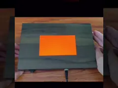
High Resolution I2C Optical Bonding 10.1 Inch Dust Resistance
Optical bonding technology: Optical bonding technology is using optical glue TP assembly LCD and touch panel together without air. It's different from traditional adhesive bonding products. For traditional adhesive bonding products, double sided adhesive is pasted around four edges, there is still air gap between touch panel and LCD. For optical bonding products, there is glue the whole surface of the LCD. Dust and fog can't go inside. And the display effect will be great.
Specification:
| 1 | Type | Projected capacitive touch panel |
| 2 | VA of cover lens | 222*124mm |
| 3 | OD of cover lens | 239.4*156.25mm |
| 4 | AA of ITO glass | 225*144.43mm |
| 5 | OD of ITO glass | 237.8*154.25mm |
| 6 | Structure | 0.7mm cover+0.7mm ITO sensor |
| 7 | Controller board | Goodix 928, 9271 |
| 8 | Working environment | -20℃-70℃ |
| 9 | Storage environment | -30℃-80℃ |
| 10 | OS supported | Android, Linux, WCE |
Features of optical bonding product:
1.Since there is no gap between LCD and touch panel after assembly, dust and fog can't go inside the module.
2.There will be low interference of LCD to touch panel.
3.Vivid and clear crystal display performance than ordinary bonding method.
4.Improved hardness, vibration resistance of TFT module
Development process of optical bonding products:
·Receive customer's LCD samples.
·Evaluate LCD structure and and check the thickness of LCD bezel sheet.
·Offer quotation for customer's confirmation.
·Samples are made for confirmation
·Trial production.
·Mass production.
Lead time
for samples
Touch panel: 15 days after PO.
Optical bonding: 3-5 days after touch panels and LCD get ready.
for mass production
Touch panel: 18 days after PO.
Optical bonding: 5-8 days after touch panels and LCD are made.
Optical bonding technology: Use optical glue to bond LCD and touch panel without air gap.
Comparison between ordinary adhesive bonding and optical bonding
Optical bonding eliminates the air gap between LCD and toch panel, which helps to reduce the light reflection by almost 75%. And it makes the module look more transparent and enhance the dispaly effect of the screen.
Engineering drawing