
Add to Cart
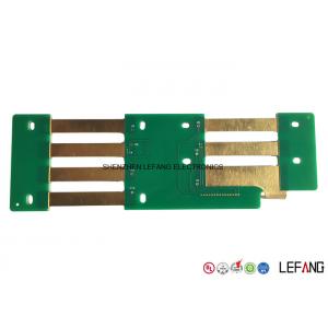
2.0 mm Copper Base PCB Circuit Board for Power Panel Motherboard with Immersion Gold
The 3.6 mm double sided 2 layers Copper Base PCB is applied for power panel. And the board size of this copper base PCB Board is 229*73 mm, with green solder mask and immersion gold ( ENIG ) surface treatment.
How to get quick quotation?
| Step 1 Please send us Gerber file with these format: .CAD / .Gerber / .PCB / .DXP / .P-CAD, etc | ||||||||||||||||||||
| Step 2 Also please provide us the below details for quick quotation: | ||||||||||||||||||||
Board material: Fr - 4 / CEM - 1 / CEM - 3 / 22F / Fr - 1 / others | ||||||||||||||||||||
| Material brand: SY / KB / Rogers (optional) | ||||||||||||||||||||
| Material Specification:High Tg / copper based / aluminum based or others (optional) | ||||||||||||||||||||
| Board thickness: 0.1 - 6.0 mm | ||||||||||||||||||||
| Copper thickness: 0.05 Oz - 8 Oz ( 17 um - 288 um ) | ||||||||||||||||||||
| Surface Treatment: OSP / ENIG / HASL / Lead Free HASL / Immersion Tin / Immersion Sin | ||||||||||||||||||||
| Color of solder mask and silk print: Green / red / blue / black / white / yellow ,etc | ||||||||||||||||||||
| Board size and quantity | ||||||||||||||||||||
If you don't have Gerber file, please provide us the imfomation as step 2 or post your PCB Board to us for clone. | ||||||||||||||||||||
SAMPLE: | ||||||||||||||||||||
| ||||||||||||||||||||
| Item | Details |
| Max layer count | 20 L |
| Max board thickness | 6.0 mm |
| Max aspect ratio | 10 : 1 |
| Max copper thickness | 6 OZ |
| Max dimension | 600 * 700mm |
| Min thickness of 4 layers PCB | 0.4 mm |
| Min hole / pad | 0.15 / 0.35mm |
| Hole location accuracy | + / - 0.05mm |
| PTH hole tolerance | + / - 0.05mm |
| Min line width and line space | 0.065 / 0.065mm |
| Surface treatment | HASL / HASL lead free, OSP Immersion gold/silver/tin, gold plating (hard gold and soft gold), silver plating, tin plating, platinum plating, carbon ink, ENEPIG (electroless nickel - electroless palladium - immersion gold) |
| Layer count | Sample lead time/workday | Batch lead time/workday |
| 1-2L | 2 | 6 |
| 4L | 5 | 8 |
| 6L | 5 | 9 |
| 8L | 6 | 10 |
| 10L | 8 | 10 |
| 12L | 8 | 12 |
| 14L | 10 | 15 |
| 16L | 10 | 18 |
| 18-40L (Up to difficulty) | at least 18 | at least 24 |
| P.S. For HDI, Blind/Buried Hole PCB: Regular Lead Time + 3 workdays | ||
| AOI (Automated Optical Inspection) | Impedance control |
| Automatic short-circuit testing | Metallographic microscope |
| RoHS detector | Fly probe/ fixture mold |
| Dielectric tester | Visual inspection |
Now send us your inquiry, and you will be replied within 8 hours!
Little knowledge - Medical Devices
Electronics contributes significantly to today's health-care industry like in diagnostic, monitoring and treatment devices. Because of the health implications associated with them, medical PCBs are held to higher standards than most other PCB types.
PCBs within the medical industry are highly specialized to satisfy the restriction of medical devices. In many medical applications, requirements like size and appearance are existed for an implant or emergency room monitor. For this reason, medical PCBs tend to be specialty high-density interconnect PCBs (HDI PCBs) or made with flexible base materials, allowing PCB to flex during use.

