2" S Doped GaP Semiconductor EPI Wafer N Type P Type 250um 300um Light-Emitting Diodes
Brand Name:ZMSH
Certification:ROHS
Model Number:GaP
Minimum Order Quantity:25pcs
Delivery Time:In 30 days
Payment Terms:T/T
Contact Now
Add to Cart
Verified Supplier
Location:
Shanghai Shanghai China
Address:
Rm5-616,No.851,Dianshanhu avenue, Qingpu area,Shanghai city,CHINA
Supplier`s last login times:
within 13 hours
Shipping
lt's easy to get a shipping quote! Just click the button below and complete the short form.
Get Shipping Quote
Product Details
Company Profile
Product Details
2” S Dopped GaP Semiconductor EPI Wafer N Type P Type 250um 300um Light-Emitting Diodes
Description:
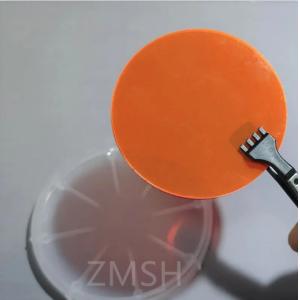
Gallium phosphide (GaP) is a group Ⅲ-V compound. The appearance is orange-red transparent crystal.Gallium phosphide is used to make inexpensive red, green and orange light-emitting diodes with low to medium brightness. Its life is shorter at high currents, and its life is also quite sensitive to temperature.Gallium phosphide (GaP) is an inorganic compound and a semiconductor material with an indirect energy gap of 2.26eV (300K). Its polycrystalline material is light orange. Gallium phosphide is odorless and does not dissolve in water.To become an N-type semiconductor, sulfur or tellurium must be doped, and to make a P-type semiconductor, zinc must be doped.
Features:
Semiconductor material Gallium phosphide referred to as Gap, is composed of gallium (Ga) and phosphorus (P) synthesis of ⅲ-ⅴ group compound semiconductor, at room temperature, its higher purity is orange red transparent solid, Gallium phosphide is an important material for the production of semiconductor visible light emitting devices, mainly used for manufacturing rectifier, transistor, light guide, laser diode and cooling elements. Gallium phosphide and gallium arsenide are semiconductors with electroluminescent properties and are the so-called third generation semiconductors after germanium and silicon. Gallium arsenide LED has high quantum efficiency, compact and simple device structure, high mechanical strength and long service life, and can be used in "optical phone".
Parameters:
| Items | Parameters |
| Colour | Transparent Orange Red |
| Diameter | 50.6+0.3 |
| Thickness | 175 225 |
| Dopant | S |
| Density | 4.138 g/cm3 |
| Melting point | 1477 °C |
| Growth method | LEC |
| Solubility | Soluble |
| Orientation | (111)A 0°+0.2 |
| Refractive index | 4.3 |
| Warp | 10um |
| Bow | 10um |
| TTV | 10um |
| Grade | A |
Application:
Indium phosphide (InP) is a III~V compound with sphalerite crystal structure, lattice constant of 5.87×10⁻¹⁰ m, band gap of 1.34 eV, and mobility of 3000~4500 cm2 / (V.S) at room temperature. InP crystals have many advantages, such as high saturated electron drift speed, strong radiation resistance, good thermal conductivity and high photoelectric conversion efficiency, and are widely used in optical communication, high-frequency millimeter wave devices, photoelectric integrated circuits and solar cells for outer space. In the future, the demand for components will link the applications of 5G communications, automotive electronics and optical communications with the characteristics of high speed, high frequency and high power, and the second and third generation compound semiconductors are expected to break through Moore's Law of silicon semiconductors.
Other product:
FAQ;
Q: What is the Brand Name of S Dopped GaP?
A: The Brand Name of S Dopped GaP is ZMSH.
Q: What is the Certification of S Dopped GaP?
A: The Certification of S Dopped GaP is ROHS.
Q: Where is the Place of Origin of S Dopped GaP?
A: The Place of Origin of S Dopped GaP is CHINA.
Q: What is the MOQ of S Dopped GaP at one time?
A: The MOQ of S Dopped GaP is 25pcs at one time.

2" S Doped GaP Semiconductor EPI Wafer N Type P Type 250um 300um Light-Emitting Diodes
Inquiry Cart
0