Product Details
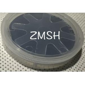
Indium Phosphide Wafer InP Semiconductor Substrates Epitaxial 2''
3'' Thickness 350um
Description of Indium Phosphide:
Indium Phosphide (InP) chips are a widely used material in
optoelectronics and semiconductor devices. It has the following
advantages:
- High electron mobility: Indium phosphide chips have a high electron
mobility, which means that electrons move faster through the
material.
- Controlled material properties: The properties of indium phosphide
wafers can be regulated by controlling the epitaxial growth process
of the material and doping techniques.
- Wide band gap: The indium phosphide wafer has a wide band gap,
enabling it to operate in the visible and infrared light ranges.
- High saturation drift speed: The indium phosphide wafer has a high
saturation drift speed, which means that the electron drift speed
reaches the maximum under a high electric field.
- Excellent thermal conductivity: The indium phosphide wafer has a
high thermal conductivity, which means that it is able to
efficiently conduct and dissipate heat, thereby improving the
reliability and performance stability of the device.
Features of Indium Phosphide:
Indium Phosphide (InP) chips have some remarkable characteristics
that make them widely used in optoelectronics and semiconductors.
The following are some of the main characteristics of indium
phosphide chip materials:
- Direct band gap: Indium phosphide has a direct band gap
characteristic that makes it excellent in optical devices.
- Wide band gap range: Indium phosphide has a wide band gap ranging
from infrared to ultraviolet spectrum.
- High electron mobility: Indium phosphide has a high electron
mobility, which makes it excellent in high-frequency electronics
and high-speed optoelectronics.
- Excellent thermal conductivity: Indium phosphide has a high thermal
conductivity and can effectively dissipate heat.
- Good mechanical and chemical stability: Indium phosphide chips have
good mechanical and chemical stability and can maintain stability
and reliability under different environmental conditions.
- Adjustable band structure: The band structure of indium phosphide
materials can be regulated by doping and alloying techniques to
meet the requirements of different devices.
Technical Parameters of Indium Phosphide:
Item | Parameter | UOM |
Material | InP |
|
Conduction type/Dopant | S-C-N/S |
|
Grade | Dummy |
|
Diameter | 100.0+/-0.3 | mm |
Orientation | (100) +/-0.5° |
|
Lamellar twin area | useful single crystal area with (100) orienation > 80% |
|
Primary Flat Orientation | EJ(0-1-1) | mm |
Primary Flat Length | 32.5+/-1 |
|
Secondary Flat Orientation | EJ(0-11) |
|
Secondary Flat Length | 18+/-1 |
|
Applications of Indium Phosphide:
Indium Phosphide (InP) wafers have a wide range of applications in
optoelectronics and semiconductor substrates:
- Optical communication: InP wafers are widely used in the field of
optical communication for high-speed optical fiber communication
systems. They are used to fabricate devices such as lasers, optical
modulators, optical receivers, optical amplifiers and optical fiber
couplers.
- Photoelectronic devices: InP wafers are used to make
photoelectronic devices such as photodiodes, photodetectors, solar
cells and photocouplers.
- High-speed electronic devices: InP substrates are widely used in
the field of high-frequency electronic devices. In particular, InP
wafes' high electron mobility transistors (HEMTs) are used to
prepare devices such as high-frequency amplifiers, RF switches and
microwave integrated circuits for applications such as wireless
communications, radar systems and satellite communications.
- Integrated optical devices: InP wafers are used to prepare
integrated optical devices such as optical waveguides, optical
modulators, optical switches and optical amplifiers.
- Photonics research: InP wafers play an important role in photonics
research. They are used in laboratory research, quantum optics,
quantum information processing and optical quantum devices.
- In addition to the above applications, InP wafers are also used in
other fields, such as optical sensing, biomedicine, light storage
and semiconductor substrates
FAQ:
Q1: What brand name is the InP wafer?
A1: The InP wafer is made by ZMSH.
Q2: What's the diameter of the InP wafer?
A2: The diameter of InP wafer is 2'', 3'', 4''.
Q3: Where is the InP wafer from?
A3: The InP wafer is from China.
Q4: Is the InP wafer ROHS certified?
A4: Yes, the InP wafer is ROHS certified.
Q5: How many InP wafes can I buy at 1 time?
A5: The minimum order quantity of the InP wafer is 5pcs.
Other products:
Silicon wafers
Company Profile
SHANGHAI FAMOUS TRADE CO.,LTD. locates in the city of Shanghai,
Which is the best city of China, and our factory is founded in Wuxi city in 2014.
We specialize in processing a varity of materials into wafers,
substrates and custiomized optical glass parts.components widely
used in electronics, optics, optoelectronics and many other fields.
We also have been working closely with many domestic and oversea
universities, research institutions and companies, provide
customized products and services for their R&D projects.
It's our vision to maintaining a good relationship of cooperation with our all
customers by our good reputatiaons.