
Add to Cart
SD
customzied size MPCVD method GaN&Diamond Heat Sink wafers for Thermal management area
Diamond has wide band gap, high thermal conductivity, high
breakdown field strength, high carrier mobility, high temperature
resistance, acid and alkali resistance, corrosion resistance,
radiation resistance and other superior properties
High power, high frequency, high temperature fields play an
important role, and are considered as one of the most promising
wide band gap semiconductor materials.
Advantages of Diamond
• Highest room temperature thermal conductivity of any material (up
to 2000W/m.k) • Surface roughness and high flatness of growth
surface<1nm can be achieved
• Electrical insulation • Extremely light weight
• High mechanical strength • • Chemical inertia and low toxicity
• Wide range of available thicknesses • Wide range of diamond
bonding solutions
Diamond is a super heat dissipation material with excellent
performance:
• Diamond has the highest thermal conductivity of any material at
room temperature. And heat is the important reason of electronic
product failure.
According to statistics, the temperature of the working junction
will drop Low 10 ° C can double the device life. The thermal
conductivity of diamond is 3 to 3 higher than that of common
thermal management materials (such as copper, silicon carbide and
aluminum nitride)
10 times. At the same time, diamond has the advantages of light
weight, electrical insulation, mechanical strength, low toxicity
and low dielectric constant, which make diamond, It is an excellent
choice of heat dissipation materials.
• Give full play to the inherent thermal performance of diamond,
which will easily solve the "heat dissipation" problem faced by
electronic power, power devices, etc.
On the volume, improve reliability and enhance power density. Once
the "thermal" problem is solved, the semiconductor will also be
significantly improved by effectively improving the performance of
thermal management,
The service life and power of the device, at the same time, greatly
reduce the operating cost.
Diamond heat sink TC1200, TC 1500, TC 1800
1.International leading grinding and polishing capability,
achieving surface roughness of growth surface Ra < 1nm
Composite deposition is an efficient and precise machining method
for diamond atomic level surface based on plasma assisted grinding
and polishing. For 2-inch diamond substrate, the surface can be
coarsened
The roughness is reduced from tens of micrometers to less than 1nm.
This technology has high removal efficiency, can obtain atomic
level flat surface, and does not produce sub surface.
Surface damage. At present, only a few manufacturers have diamond
super surface grinding and polishing to Ra < 1nm, and the chemical
composite has reached the international leading level.
2.Ultra high thermal conductivity, T C:1000-2000 W/m.K
When the thermal conductivity is required to be 1000~2000 W/m K,
diamond heat sink is the preferred and only optional heat sink
material. Composite SMT can be determined according to customer
requirements
At present, three standard products have been launched: TC1200, TC
1500 and TC 1800.
3. Provide customized services such as thickness, size and shape
The thickness of the composite deposited diamond heat sink can
range from 200 to 1000 microns, and the diameter can reach 125 mm
in the first half of 2022. We have laser cutting and polishing
capabilities to provide customers with geometric shape, surface
flatness and low roughness, as well as metallization services that
meet their specific requirements.
Typical Applications
High power RF device
• Base station RF amplifier • Satellite RF uplink amplifier •
Microwave amplifier
High power photoelectric
• Laser diode and laser diode array • Optical plane IC module •
High brightness LED
High voltage power device
• Automotive subsystem • Aerospace subsystem • Energy distribution
• DC/DC converter
Semiconductor equipment
• Characterization testing • Patch process
Size specification Detail
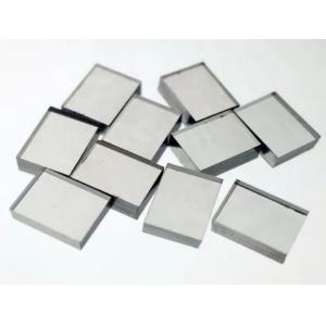
Products Show

