Product Details
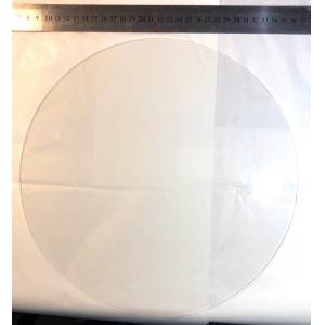
ultrathin sapphire glass wafer ,4inch 0.5mm C-axis sapphire wafer
for epi-ready,sapphire thick glass lens for covering,sapphire
optical windows,4inch 0.3mm thickness sapphire wafer,
diameter300mm 12inch double side polished sapphire glass wafers
window with notch for semiconductor carrier wafer
Chemically, sapphire is single crystal aluminum oxide (Al2O3), and
is useful in a transmission range from 0.2 - 5.5µm.Sapphire , so
making them ideal materials for demanding applications (such as
laser systems) because of their extreme surface hardness, high
thermal conductivity, high dielectric constant and resistance to
common chemical acids and alkalis. And sapphire also is the second
hardest crystal next to diamonds and, because of their structural
strength, sapphire windows can be made much thinner than other
common dielectric windows with improved transmittance.-------------------------------------------------------------------------------------
We can supply professional customized service in time and provide
cooperation and support of new product development and technology
appliance.
Material Sapphire(Al2O3)
Density(20°C) Kg/m3 3.98×10³
Crystal Structure hexagonal
Crystal lattice constant a=4.785Å c=12.991 Å
Mohs hardness 9
Melting Point 2045°C
Boiling Point 3000°C
Coefficient of Thermal Expansion α=5.8×10 -6 /K
Specific heat 0.418W.s/g/k
Thermal conductio 25.12W/m/k(@100°C)
Refractive Index (nd) no=1.768ne=1.76
dn/dt 13×10-6/K(@633nm)
Tranmission T≈85%(0.3~5um)
Permittivity 11.5(//c), 9.3(⊥c)
ApplicationsSapphire Washers, Sapphire Windows, Sapphire Bearings, Sapphire
Rods, Sapphire Tubes, Ruby
sapphire wafer, dome sapphire, Sapphire insulation Film, Sapphire
ball lens, Sapphire/ruby ball
Specification for 12inch wafers
- 12inch 1.5mm thickness sapphire wafer specification
- Material: Single crystal Al2O3 99.999%
- Orientation: C-plane(0001) Off M -axis 0.2°±0.1
- Diameter:300±0.3mm;
- Thickness 1500um,
- Primary flat:: V-notch
- OF Orientation flat: A axis±0.1°
- Frontside Surface Roughness:Ra<0.3nm
- Backside Surface Roughness: <0.3nm
- TTV:<40um BOW:-30um WARP:<60um
- Laser Mark Series No. by needs
- Package:Vacuum-sealed containers with nitrogen backfill in a class
100 environment
- Cleanliness :Free visible contamination
Sapphire Wafer Process Step
we also can provide other materials crystal seimconductor wafers as
like GaN, SiC,GaAs,InP,MgO etc.
Packing Details : Packing, BOX,CARTONS by 25pcs cassette in
cleaning room by vacuumize
Delivery Details : 3-20 days after order of Solid bicycle tire
tubesrecieving your pament will be send out.
Company Profile
SHANGHAI FAMOUS TRADE CO.,LTD. locates in the city of Shanghai,
Which is the best city of China, and our factory is founded in Wuxi city in 2014.
We specialize in processing a varity of materials into wafers,
substrates and custiomized optical glass parts.components widely
used in electronics, optics, optoelectronics and many other fields.
We also have been working closely with many domestic and oversea
universities, research institutions and companies, provide
customized products and services for their R&D projects.
It's our vision to maintaining a good relationship of cooperation with our all
customers by our good reputatiaons.