
Add to Cart
2inch 3inch 4inch InP substrates for LD application, semiconductor wafer,InP wafer,single crystal wafer
InP introduce
| InP single crystal | |
The tCZ growth (modified Czochralski method) is used to pull a
single crystal through a boric oxide liquid encapsulant starting
from a seed. The dopant (Fe, S, Sn or Zn) is added to the crucible
along with the polycrystal. High pressure is applied inside the
chamber to prevent decomposition of the Indium Phosphide. we has developed a process to yield fully stoechiometric, high purity
and low dislocation density InP single crystal. | |
Specification
| Item | Diameter | Type | carrying concentration | Mobility | Resistivity | MPD |
| S-InP | 2 | N | (0.8-6)X10^18 | (1.5-3.5)x10^3 | <500 | |
| 3 | <500 | |||||
| 4 | <1x10^3 | |||||
| Fe-InP | 2/3/4 | SI | >1000 | >0.5x10^7 | >5x10^3 | |
| Zn-InP | 2/3/4 | P | (0.6-6)X10^18 | 50-70 | <1x10^3 | |
| No dope InP | 2 | N | <3x10^16 | (3.5-4)x10^3 | <5x10^3 | |
| Other | ||||||
| Orientation | (100)/(111)±0.5° | Flatness | ||||
| TTV | Bow | Warp | ||||
| <12um | <12um | ≤15um | ||||
| 1st OF Flat | 16±2mm | 22±2mm | 32.5±2.5mm | |||
| 2st OF Flat | 8±1mm | 11±2mm | 32.5±2.5mm | |||
| Surface:1sp or 2sp ,2inch 350±25um,3inch 600±25um,4inch 625±25um,or by customized | ||||||
2. InP Wafer process step
| InP Wafer processing | |
| Each ingot is cut into wafers which are lapped, polished and surface prepared for epitaxy. The overall process is detailed hereunder. | |
| Flat specification and identification | The orientation is indicated on the wafers by two flats (long flat for orientation, small flat for identification). Usually the E.J. standard (European-Japanese) is used. The alternate flat configuration (U.S.) is mostly used for Ø 4" wafers. |
| Orientation of the boule | Either exact (100) or misoriented wafers are offered. |
| Accuracy of the orientation of OF | In response to the needs of the optoelectronic industry, we offers wafers with excellent accuracy of the OF orientation : < 0.02 degrees. This feature is an important benefit to customers making edge-emitting lasers and also to manufacturers who cleave to separate dies allowing their designers to reduce the real-estate wasted in the streets. |
| Edge profile | There are two common specs : chemical edge processing or mechanical edge processing (with an edge grinder). |
| Polishing | Wafers are polished by means of a chemical-mechanical process resulting in a flat, damage-free surface.we provides both double-side polished and single-side polished (with lapped and etched back side) wafers. |
| Final surface preparation and packaging | Wafers go through many chemical steps to remove the oxide produced
during polishing and to create a clean surface with stable and
uniform oxide layer that is ready for epitaxial growth - epiready
surface and that reduces trace elements to extremely low levels .
After final inspection, the wafers are packaged in a way that
maintains the surface cleanliness. Specific instructions for oxide removal are available for all types of epitaxial technologies (MOCVD, MBE). |
| Database | As part of our Statistical Process Control/Total Quality Management Program, extensive database recording the electrical and mechanical properties for every ingot as well as crystal quality and surface analysis of wafers are available. At each stage of fabrication, the product is inspected before passing to the next stage to maintain a high level of quality consistency from wafer to wafer and from boule to boule. |
Sample
QC. standard
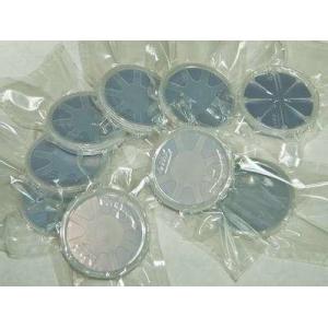
Package & delivery
FAQ:
Q: What's your MOQ?
A: (1) For inventory, the MOQ is 5 pcs.
(2) For customized products, the MOQ is 10-30 pcs up.
Q: What's the way of shipping and cost?
A:(1) We accept DHL, Fedex, EMS etc.
(2) If you have your own express account, it's great.If not,we could help you ship them.
Freight is in accordance with the actual settlement.
Q: How to pay?
A: T/T, Paypal, Secure payment and Assurance payment.
Q: What's the delivery time?
A: (1) For the standard products
For inventory: the delivery is 5 workdays after you place the order.
For customized products: the delivery is 2 or 3 weeks after you place the order.
(2) For the special-shaped products, the delivery is 4 workweeks after you place the order.
Q: Do you have standard products?
A: Our standard products in stock.
Q: Can I customize the products based on my need?
A: Yes, we can customize the material, specifications for your optical components based on your needs.

