Undoped Semi - Insulating Gallium Nitride Wafer HVPE And Template Type
Brand Name:zmsh
Model Number:GaN-001
Minimum Order Quantity:1pcs
Delivery Time:2-4weeks
Payment Terms:L/C, , T/T
Place of Origin:CHINA
Contact Now
Add to Cart
Verified Supplier
Location:
Shanghai Shanghai China
Address:
Room.1-1805,No.1079 Dianshanhu Road,Qingpu Area Shanghai city, China /201799
Supplier`s last login times:
within 13 hours
Product Details
Company Profile
Product Details
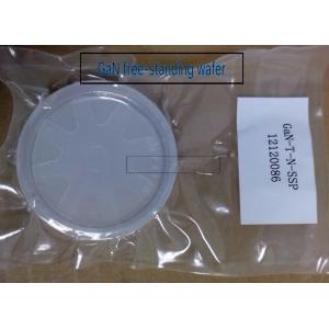
2inch HVPE method Gallium Nitride GaN wafer ,free standing GaN substrates for LD,10x10mm size GaN chips,HVPE GaN wafer
About GaN Feature Introduce
The growing demand for high-speed, high-temperature and high power-handling capabilities has made the semiconductor industry rethink the choice of materials used as semiconductors. For instance, as various faster and smaller computing devices arise, the use of silicon is making it difficult to sustain Moore’s Law. But also in power electronics, So GaN semiconductor wafer is grown out for the need. Due to its unique characteristics (high maximum current, high breakdown voltage, and high switching frequency), Gallium Nitride GaN is the unique material of choice to solve energy problems of the future. GaN based systems have higher power efficiency, thus reducing power losses, switch at higher frequency, thus reducing size and weight. GaN technology is used in numerous high-power applications such as industrial, consumer and server power supplies, solar, AC drive and UPS inverters, and hybrid and electric cars. Furthermore, GaN is ideally suited for RF applications such as cellular base stations, radars and cable TV infrastructure in the networking, aerospace and defense sectors, thanks to its high breakdown strength, low noise figure and high linearity. |
| 2”GaN Substrates | ||
| Item | GaN-FS-N | GaN-FS-SI |
| Dimensions | Ф 50.8mm ± 1mm | |
| Marco Defect Density | A Level | ≤ 2 cm-2 |
| B Level | > 2 cm-2 | |
| Thickness | 330 ± 25 µm | |
| Orientation | C-axis(0001) ± 0.5° | |
| Orientation Flat | (1-100) ± 0.5°, 16.0 ± 1.0mm | |
| Secondary Orientation Flat | (11-20) ± 3°, 8.0 ± 1.0mm | |
| TTV(Total Thickness Variation) | ≤15 µm | |
| BOW | ≤20 µm | |
| Conduction Type | N-type | Semi-Insulating |
| Resistivity(300K) | < 0.5 Ω·cm | >106 Ω·cm |
| Dislocation Density | Less than 5x106 cm-2 | |
| Useable Surface Area | > 90% | |
| Polishing | Front Surface: Ra < 0.2nm. Epi-ready polished | |
| Back Surface: Fine ground | ||
| Package | Packaged in a class 100 clean room environment, in single wafer containers, under a nitrogen atmosphere. | |
Applications
- - Various LED's: white LED, violet LED, ultraviolet LED, blue LED
- - Laser diodes: violet LD, green LD for ultra small projectors.
- - Power electronic devices
- - High frequency electronic devices
- - Environmental detection
- ■ Usage
- Substrates for epitaxial growth by MOCVD etc.


Undoped Semi - Insulating Gallium Nitride Wafer HVPE And Template Type
Inquiry Cart
0