3 Inch Silicon Carbide Wafer , Sic Substrate Excellent Transient Characteristics
Brand Name:zmkj
Model Number:4inch--semi high purity
Minimum Order Quantity:1pcs
Delivery Time:15days
Place of Origin:china
Price:by required
Contact Now
Add to Cart
Verified Supplier
Location:
Shanghai Shanghai China
Address:
Room.1-1805,No.1079 Dianshanhu Road,Qingpu Area Shanghai city, China /201799
Supplier`s last login times:
within 13 hours
Product Details
Company Profile
Product Details
3inch sic wafer,4H High Purity Silicon Carbide Substrates,high purity 4inch SiC substrates ,4inch Silicon Carbide substrates for semiconductor, 4inch SiC substrates ,Silicon Carbide substrates for semconductor ,sic single crystal wafers ,sic ingots for gem
Application areas
1 high frequency and high power electronic devices Schottky diodes, JFET, BJT, PiN, diodes, IGBT, MOSFET
2 optoelectronic devices: mainly used in GaN/SiC blue LED substrate material (GaN/SiC) LED
advantagement
• Low lattice mismatch
• High thermal conductivity
• Low power consumption
• Excellent transient characteristics
• High band gap
Silicon Carbide SiC crystal substrate wafer carborundum
SILICON CARBIDE MATERIAL PROPERTIES
| Property | 4H-SiC, Single Crystal | 6H-SiC, Single Crystal |
| Lattice Parameters | a=3.076 Å c=10.053 Å | a=3.073 Å c=15.117 Å |
| Stacking Sequence | ABCB | ABCACB |
| Mohs Hardness | ≈9.2 | ≈9.2 |
| Density | 3.21 g/cm3 | 3.21 g/cm3 |
| Therm. Expansion Coefficient | 4-5×10⁻⁶/K | 4-5×10⁻⁶/K |
| Refraction Index @750nm | no = 2.61 ne = 2.66 | no = 2.60 ne = 2.65 |
| Dielectric Constant | c~9.66 | c~9.66 |
| Thermal Conductivity (N-type, 0.02 ohm.cm) | a~4.2 W/cm·K@298K c~3.7 W/cm·K@298K | |
| Thermal Conductivity (Semi-insulating) | a~4.9 W/cm·K@298K c~3.9 W/cm·K@298K | a~4.6 W/cm·K@298K c~3.2 W/cm·K@298K |
| Band-gap | 3.23 eV | 3.02 eV |
| Break-Down Electrical Field | 3-5×10⁶V/cm | 3-5×10⁶V/cm |
| Saturation Drift Velocity | 2.0×10⁵m/s | 2.0×10⁵m/s |
2. substrates size of standard
| 3 inch Diameter 4H Silicon Carbide Substrate Specifications | ||||
| SUBSTRATE PROPERTY | Ultra Grade | Production Grade | Research Grade | Dummy Grade |
| Diameter | 76.2 mm ±0.38 mm | |||
| Surface Orientation | on-axis: {0001} ± 0.2°; off-axis: 4°toward <11-20> ± 0.5° | |||
| Primary Flat Orientation | <11-20> ± 5.0 ̊ | |||
| Secondary Flat Orientation | 90.0 ̊ CW from Primary ± 5.0 ̊, silicon face up | |||
| Primary Flat Length | 22.0 mm ± 2.0 mm | |||
| Secondary Flat Length | 11.0 mm ± 1.5mm | |||
| Wafer Edge | Chamfer | |||
| Micropipe Density | ≤1 micropipes/ cm2 | ≤5 micropipes/ cm2 | ≤10 micropipes/ cm2 | ≤50 micropipes/ cm2 |
| Polytype areas by high-intensity light | None permitted | ≤10% area | ||
| Resistivity | 0.015 Ω·cm~0.028 Ω·cm | (area 75%)0.015Ω·cm~0.028 Ω·cm | ||
| Thickness | 350.0 μm ± 25.0 μm or 500.0 μm ± 25.0 μm | |||
| TTV | ≤10 μm | ≤15 μm | ||
| Bow(absolute value) | ≤15 μm | ≤25 μm | ||
| Warp | ≤35 μm | |||
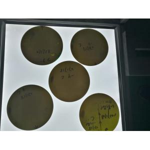
3.sample
FAQ:
Q: What's the way of shipping and cost and pay term ?
A:(1) We accept100% T/T In advance by DHL, Fedex, EMS etc.
(2) If you have your own express account, it's great.If not,we could help you ship them.
Freight is in accordance with the actual settlement.
Q: What's your MOQ?
A: (1) For inventory, the MOQ is 2pcs.
(2) For customized products, the MOQ is 25pcs up.
Q: Can I customize the products based on my need?
A: Yes, we can customize the material, specifications and shape, size based on your needs.
Q: What's the delivery time?
A: (1) For the standard products
For inventory: the delivery is 5 workdays after you place the order.
For customized products: the delivery is 2 or 3 weeks after you place the order.
(2) For the special-shaped products, the delivery is 4 workweeks after you place the order.


3 Inch Silicon Carbide Wafer , Sic Substrate Excellent Transient Characteristics
Inquiry Cart
0