
Add to Cart
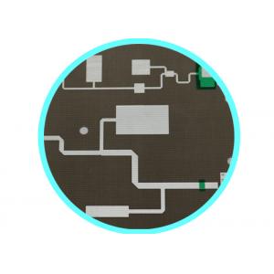
PCB Audio Amplifier RF Transceiver Taconic High Frequency PCB
Double Layer 1oz Electronic Circuit
Quick detail:
| Origin:China | Special: Taconic material |
| Layer:4 | Thickness:0.79mm |
| Surface: ENIG | Hole:0.8 |
Specification:
PCB Audio Amplifier RF Transceiver Taconic High Frequency PCB
Double Layer 1oz Electronic Circuit TACONIC high-performance
insulating material for microwave, radio frequency (RF) and
high-speed digital signal processing (DSP) market with PTFE/type
woven glass fiber fabric sheet.This material can be applied to LNAs
LNBs, PCS/PCN antenna system, global positioning system (GPS) and
UMTS antenna system,And the power amplifier, passive components,
collision avoidance radar system, aviation help guide remote
control technology and system of the phased array radar.
Taconic materials are UL 94V-0 rated for active devices and high
power RF designs.
High Speed Design Frequency PCB Board Special high electromagnetic frequency circuit boards, in general,
can be defined as the frequency of the high frequency of 1GHz. Its
physical properties, precision, technical parameters required is
very high, commonly used in automotive anti-collision systems,
satellite systems, radio systems, etc.
The basic characteristics of a high frequency board material
requirements are the following:
(1) dielectric constant (Dk) must be small and very stable, usually
the smaller the better signal transfer rate and the dielectric
constant of the material
Inversely proportional to the square root of high dielectric
constant is likely to cause the signal propagation delay.
(2) the dielectric loss (Df) must be small, mainly affect the
quality, the smaller the dielectric loss signal transmission of the
signal loss is smaller.
(3) as far as possible consistent with the coefficient of thermal
expansion of the copper foil, copper foil separated because of
inconsistency will cause changes in the hot and cold.
(4) to low water absorption, high water absorption will affect the
dielectric constant and dielectric loss when damp.
(5) Other heat resistance, chemical resistance, impact strength,
peel strength, etc. must also be good.
Typical Applications
Microwave Antenna 4 Layer PCB Board,Radio frequency (RF) and microwave PCB’s are a type of PCB designed
to operate on signals in the megahertz to gigahertz frequency
ranges (medium frequency to extremely high frequency). These
frequency ranges are used for communication signals in everything
from cellphones to military radars. The materials used to construct
these PCB’s are advanced composites with very specific
characteristics for dielectric constant (Er), loss tangent, and CTE
(co-efficient of thermal expansion).
High frequency circuit materials with a low stable Er and loss
tangent allow for high speed signals to travel through the PCB with
less impedance than standard FR-4 PCB materials. These materials
can be mixed in the same Stack-Up for optimal performance and
economics.
Parameter:
| o | Item | Data |
| 1 | Layer: | 1 to 24 layers |
| 2 | Material type: | FR-4, CEM-1, CEM-3, High TG, FR4 Halogen Free, Rogers |
| 3 | Board thickness: | 0.20mm to 3.4mm |
| 4 | Copper thickness: | 0.5 OZ to 4 OZ |
| 5 | Copper thickness in hole: | >25.0 um (>1mil) |
| 6 | Max. Board Size: | (580mm×1200mm) |
| 7 | Min. Drilled Hole Size: | 4mil(0.1mm) |
| 8 | Min. Line Width: | 3mil (0.075mm) |
| 9 | Min. Line Spacing: | 3mil (0.075mm) |
| 10 | Surface finishing: | HASL / HASL lead free, HAL, Chemical tin, Chemical Gold, Immersion Silver/Gold, OSP, Gold plating |
| 11 | Solder Mask Color: | Green/Yellow/Black/White/Red/Blue |
| 12 | Shape tolerance: | ±0.13 |
| 13 | Hole tolerance: | PTH: ±0.076 NPTH: ±0.05 |
| 14 | Package: | Inner packing: Vacuum packing / Plastic bag,Outer packing: Standard carton packing |
| 15 | Certificate: | UL,SGS,ISO 9001:2008 |
| 16 | Special requirements: | Buried and blind vias+controlled impedance +BGA |
| 17 | Profiling: | Punching, Routing, V-CUT, Beveling |

