
Add to Cart
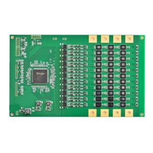
Flexible Double-layer PCB Board Soldering SMT Patch Processing High-frequency
Double-sided PCB board is a very important PCB board in the circuit board, the market has double-sided circuit board metal base PCB board, Hi-Tg heavy copper foil circuit board, flat winding double-sided circuit board, high frequency PCB, mixed dielectric base high frequency double-sided circuit board, etc. It is suitable for a wide range of high-tech industries such as: telecommunications, power supply, computer, industrial control, digital products, scientific and educational instruments, medical instruments, automobiles, aerospace defense and so on.
The difference between double-sided PCB board and single-sided PCB board is that the single-panel circuit is only on one side of the PCB board, while the double-sided PCB circuit can be in the two sides of the PCB board, with holes in the middle to connect the double-sided PCB board circuit. Parameters of double-sided PCB board In addition to the production process of double-sided PCB board is different from that of single-sided PCB board, there is also a copper sinking process, that is, the process of double-sided circuit conduction.
| Copper Thickness | 1oz~3oz,0.5-5 Oz |
| Board Thickness | 1.6mm, 0.5~3.2mm, 0.2-3.0mm, 0.3~2.5mm, 2.0mm |
| Min. Hole Size | 0.25mm, 0.1mm, 0.2 Mm, 0.15-0.2mm, 0.1mm-1mm |
| Min. Line Spacing | 0.003", 4mil, 0.2mm, 0.15mm, 0.1mm4mil) |
| Application | Electronics Device, Consumer Electronics, Electronical Products, Industrial, And So On |
| Layer | 1~20 Layers, 1-24layers |
| Base Material | FR4, Aluminium, TG, Rogers, CEM-1 |
| Min. Line Width | 3mi, 4mil, 0.1mm, 0.1mm(Flash Gold)/0.15mm(HASL), 0.1 0mm |
| Surface Finishing | HASL, OSP, ENIG, HASL Lead Free, Immersion Gold |
| Product Name | Printed Circuit Board, 94V0 PCB Design / PCB Manufacturing |
| Solder Mask | Blue, Green. Red. Blue. White. Black.Yellow, Green/black/white/red/blue Etc., |
| Rohs | Lead free |
| Turnkey PCBA | PCB+components sourcing+assembly+package | ||||
| Assembly details | SMT and Thru-hole, ISO lines | ||||
| Lead Time | Prototype: 15 work days. Mass order: 20~25 work days | ||||
| Testing on products | Flying Probe Test, X-ray Inspection, AOI Test, functional test | ||||
| Quantity |
| ||||
| Files we need | PCB: Gerber files(CAM, PCB, PCBDOC) | ||||
| Files we need | Components: Bill of Materials(BOM list) | ||||
| Files we need | Assembly: Pick-N-Place file | ||||
| PCB panel Size | Min size: 0.25*0.25 inches(6*6mm) | ||||
| Max size: 20*20 inches(500*500mm) | |||||
| PCB Solder Type | Water Soluble Solder Paste, RoHS lead free | ||||
| Components details | Passive Down to 0201 size | ||||
| Components details | BGA and VFBGA | ||||
| Components details | Leadless Chip Carriers/CSP | ||||
| Components details | Double-sided SMT Assembly | ||||
| Components details | Fine Pitch to 0.8mils | ||||
| Components details | BGA Repair and Reball | ||||
| Components details | Part Removal and Replacement | ||||
| Component package | Cut Tape,Tube,Reels,Loose Parts | ||||
| PCB assembly | Drilling-----Exposure-----Plating-----Etaching & Stripping-----Punching-----Electrical Testing-----SMT-----Wave Soldering-----Assembling-----ICT-----Function Testing-----Temperature & Humidity Testing | ||||