High Density Interconncection Multilayer Circuit Board 0.05mm NPTH Tolerance
Brand Name:JINGXIN
Certification:UL, Rohs
Model Number:JX18112722
Minimum Order Quantity:1 PC
Delivery Time:5-7 days
Payment Terms:L/C, D/A, D/P, T/T, Western Union, MoneyGram
Contact Now
Add to Cart
Active Member
Location:
Shenzhen Guangdong China
Address:
F2 Building 13, F1/F2 Building 17 Hongfa Industrial Park, Tangtou Road, Shiyan, Baoan District, Shenzhen, China
Supplier`s last login times:
within 48 hours
Shipping
lt's easy to get a shipping quote! Just click the button below and complete the short form.
Get Shipping Quote
Product Details
Company Profile
Product Details
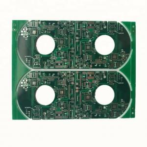
High density interconncection Multilayer PCB Board Supplier in China
Multilayer PCB board
Welcome to JINGXIN
SHENZHEN OEM ONE-STOP ELECTRONIC ASSEMBLY MANUFACTURER
We strive to provide the best contract manufacturing services
UL 94V0 Certificated Multilayer Printed Circuit Board PCB Board Assembly
As Far As 15 days for the PCBA Samples.
JINGXIN PCB&PCBA Contract Manufacturing Services Including Blows:
v Fast PCB Fabrication for Samples and Mass Production
v Electronic Components Sourcing Services
v PCBA Assembly Services:SMT,DIP,BGA...
v Function Test
v Stencil,Cable and Enclosure Assembly
v Reverse engineering service
v Standard Packing and On time Delivery
Production line process
Blank PCB
Material Cutting→Drilling→PTH→Photo process→Circuit
Exposure→Etching→Touch up→Pannel plating→Plug hole→Print Solder
mask ink→Surface Finish→Profile→Punch/V-cut→E-testing→→Final Visual
Inspection→Packing
PCB Capacity
| PCB General Capability | |
| Number of Layer | 1 - 18 Layer |
| Maximum Processing Area | 680 × 1000MM |
| Min Board Thickness | 2 Layer - 0.3MM ( 12 mil ) |
| 4 Layer - 0.4MM ( 16 mil ) | |
| 6 Layer - 0.8MM ( 32 mil ) | |
| 8 Layer - 1.0MM ( 40 mil) | |
| 10 Layer - 1.1MM ( 44 mil ) | |
| 12 Layer - 1.3MM ( 52 mil ) | |
| 14 Layer - 1.5MM ( 59 mil ) | |
| 16 Layer - 1.6MM ( 63 mil ) | |
| 18 Layer - 1.8MM ( 71 mil ) | |
| Finished Board Thickness Tolerance | Thickness ≤ 1.0MM, Tolerance: ± 0.1MM |
| 1.0MM ≤ Thickness ≤ 6.5MM, Tolerance ± 10% | |
| Twisting and Bending | ≤ 0.75%, Min: 0.5% |
| Range of TG | 130 - 215 ℃ |
| Impedance Tolerance | ± 10%, Min: ± 5% |
| Hi-Pot Test | Max: 4000V/10MA/60S |
| Surface Treatment | HASL, With Lead, HASL Free Lead |
| Flash Gold, Immersion Gold | |
| Immersion Silver, Immersion Tin | |
| Gold Finger, OSP | |
| PCB Cu Thickness + Plating | |
| Out Layer Cu Thickness | 1 - 6OZ |
| Inner Layer Cu Thickness | 0.5 - 4OZ |
| Cu Thickness of PTH | 20UM ≤ Average ≤ 25UM |
| Min: 18UM | |
| HASL with Lead | Tin 63% Lead 37% |
| HASL Free Lead | 7UM ≤ Surface Thickness ≤ 12UM |
| Thick Gold Plating | Ni Thickness: 3 - 5UM ( 120u" - 200u" ) |
| Gold Thickness: 0.025 - 1.27UM ( 1u" - 50u" ) | |
| Immersion Gold | Ni Thckness: 3 - 5UM ( 120u" - 200u" ) |
| Gold Thickness: 0.025 - 0.15UM ( 1u" - 3u" ) | |
| Immersion Silver | Ag Thickness: 0.15- 0.75 UM ( 6u" - 30u" ) |
| Gold Finger | Ni Thickness: 3 - 5UM ( 120u" - 160u" ) |
| Gold Thickness: 0.025 - 1.51UM ( 1u" - 60u" ) | |
| U940 PCB Pattern Limit Capability | |
| Min Width | 0.075MM ( 3 mil ) |
| Min Trace | 0.075MM ( 3 mil ) |
| Min Width of Ring ( Inner Layer ) | 0.15MM ( 6 mil ) |
| Min Width of Ring ( Out Layer ) | 0.1MM ( 4 mil ) |
| Min Solder Bridge | 0.1MM ( 4 mil ) |
| Min Height of Legend | 0.7MM ( 28 mil ) |
| Min Width of Legend | 0.15MM ( 6 mil ) |
| PCB Holes Processing Capability | |
| Final Hole Size | Min: Laser 0.1MM, Machine 0.2MM |
| Drilling Hole Size | 0.10 - 6.5MM |
| Drilling Tolerance | NPTH: ±0.05MM, PTH: ±0.075MM |
| Final Hole Size Tolerance ( PTH ) | φ0.20 - 1.60MM ± 0.075MM |
| φ1.60 - 6.30MM ± 0.10MM | |
| Final Hole Size Tolerance ( NPTH ) | φ0.20 - 1.60MM ± 0.05MM |
| φ1.60 - 6.50MM ± 0.05MM | |
| Drilling Strip Hole | -0L ~tu.'gth /width 2:1 |
| Min Strip Hole Width 0.65MM | |
| Length & Width Tolerance ± 0.05MM | |
| Board Thickness / Hole Size | ≤ 10:1 |
| PCB Cover Thickness Capability | |
| Solder Mask Color | Green,Matte Green,Yellow,Blue,Red,Black,Matte Black,White |
| Solder Mask Thickness | Surface Line ≥ 10UM |
| Surface Line Corner ≥ 6UM | |
| Surface Board 10 - 25UM | |
| Solder Mask Bridge Width | |
| Legend Color | White,Yellow,Black |
| Min Height of Legend | 0.70MM ( 28 mil ) |
| Min Width of Legend | 0.15MM ( 6 mil ) |
| Blue Gel Thickness | 0.2 - 1.5MM |
| Blue Gel Tolerance | ±0.15MM |
| Carbon Print Thickness | 5 - 25UM |
| Carbon Print Min Space | 0.25MM |
| Carbon Print Impedance | 200Ω |
| Blind/Burried/Half Via PCB Capability | |
| Parameters | (1+1)e.g. (4-layer)blind via:1-2,2-4 (6-layer)buried via:2-3,3-4 (8-layer)blind/buried:1-3,4-5,6-8 |
| Min Via | Laser 0.1MM, Machine 0.2MM |
| Half Via | Min: 0.6MM |
| Impedance Capability | |
| Resistance Value | Single-ended 50 - 75Ω, Difference 100Ω, Coplanar 50 - 75Ω |
PCB Photos

High Density Interconncection Multilayer Circuit Board 0.05mm NPTH Tolerance
Inquiry Cart
0