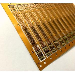
PI Material Flexible Printed Circuit Board Double Sides 2.0oz Copper Thickness
Brand Name:Jingxin
Certification:UL,RoHS, CE
Model Number:JX18112757
Minimum Order Quantity:1 pc
Place of Origin:China
Price:Negotiable
Contact Now
Add to Cart
Active Member
Location:
Shenzhen Guangdong China
Address:
F2 Building 13, F1/F2 Building 17 Hongfa Industrial Park, Tangtou Road, Shiyan, Baoan District, Shenzhen, China
Supplier`s last login times:
within 48 hours
Shipping
lt's easy to get a shipping quote! Just click the button below and complete the short form.
Get Shipping Quote
Product Details
Company Profile
Product Details
PI Material FPC double sides 2.0oz copper thickness flexible pcb
Number of layers: 2 layers
Material: FPC
Board thickness: 1.6mm
Surface plating: ENIG
Min Trace: 3mil
Silkscreen:White
With 14+ years of experience exporting PCBs overseas, We
understands the needs of your business and welcomes the opportunity
to serve you.
JINGXIN Company philosophy is simple- Deliver quality printed circuit
boards on time.
We are ISO 9001:2008 certified.
Our dedication to building a quality product is the centerpiece of
our business policy.
We are committed to fulfilling our customers' on-going quality
requirements through continuous improvements to all of our internal
processes. Our quality management system ensures the highest
operating standards at all levels.
| Item | Mass production | Small batch production | ||
| Number of layers | UP TO 18L | UP TO L | ||
| Laminate type | FR-4, halogen free, high TG(Shengyi, KB), Cem-3, PTFE, aluminum based, PTEE, Rogers or more. | FR-4, Halogen free, High TG(Shengyi, KB), Cem-3, PTFE, Aluminum based, PTEE, Rogers or more. | ||
| Maximum board size | 610mm*1100mm | 610mm*1100mm | ||
| Board thickness | 0.1mm-7.00mm | <0.1mm and >7.00mm | ||
| Minimum line width/space | 3.5mil(0.0875mm) | 3mil(0.075mm) | ||
| Minimum line gap | +/-15% | +/-10% | ||
| Outer layer copper thickness | 35um-175um | 35um-210um | ||
| Inner layer copper thickness | 12um-175um | 12um-210um | ||
| Drilling hole size(Mechanical) | 0.15mm-6.5mm | 0.15mm-6.5mm | ||
| Finished hole size (Mechanical) | 0.15mm-6.0mm | 0.15mm-6.0mm | ||
| Board thickness hole size ratio | 14:1 | 16:1 | ||
| Board thickness tolerance(t=0.8mm) | ±8% | ±5% | ||
| Board thickness tolerance(t<0.8mm) | ±10% | ±8% | ||
| Min. grid line width | 4mil(12, 18, 35um), 6mil(70um) | 4mil(12, 18, 35um), 6mil(70um) | ||
| Min. grid spacing | 6mil(12, 18, 35um), 8mil(70um) | 6mil(12, 18, 35um), 8mil(70um) | ||
| Hole size tolerance(Mechanical) | 0.05-0.075mm | 0.05mm | ||
| Hole position tolerance(Mechanical) | 0.005mm | 0.005mm | ||
| Solder mask color | Green, Blue, Black, White, Yellow, Red, Grey etc. | Green, Blue, Black, White, Yellow, Red, Grey etc. | ||
| Impedance control tolerance | +/-10% | +/-8% | ||
| Min. distance between drilling to conductor(non-blind buried orifice) | 8mil(8L), 9mil(10L), 10mil(14L), 12mil(26L) | 6mil(8L), 7mil(10L), 8mil(14L), 12mil(26L) | ||
| Min. Character width and height(35um base copper) | Line width: 5mil Height: 27mil | Line width: 5mil; height: 27mil | ||
| Max. test voltage | 500V | 500V | ||
| Max. test current | 200mA | 200mA | ||
Surface treatment | Flash Gold | 0.025-0.075um | 0.025-0.5um | |
| Immersion Gold | 0.05-0.1um | 0.1-0.2um | ||
| Sn/Pb HASL | 1-70um | 1-70um | ||
| Lead-free HASL | 1-70um | 1-70um | ||
| Immersion Silver | 0.08-0.3um | 0.08-0.3um | ||
| OSP | 0.2-0.4um | 0.2-0.4um | ||
| Gold Finger | 0.375um | >=1.75um | ||
| Hard Gold Plating | 0.375um | >=1.75um | ||
| Immersion Sin | 0.8um | |||
| V-Cut rest thickness tolerance | ±0.1mm | ±0.1mm | ||
Outline profile | Chamfer | The angle type of the chamfer | 30,45,60 | |
| Plug via hole | Max.size can be plugged | 0.6mm | ||
| Largest NPTH hole size | 6.5mm | >6.5mm | ||
| Largest PTH hole size | 6.5mm | >6.5mm | ||
| Min. solder spacer ring | 0.05mm | 0.05mm | ||
| Min. solder bridge width | 0.1mm | 0.1mm | ||
| Drilling diameter | 0.15mm-0.6mm | 0.15mm-0.6mm | ||
| Min. pad diameter with hole | 14mil( 0.15mm drilling) | 12mil( 0.1mm laser) | ||
| Min. BGA pad diameter | 10mil | 8mil | ||
| Chemical ENIG gold thickness | 0.025-0.1um(1-4U) | 0.025-0.1um | ||
| Chemical ENIG nickel thickness | 3-5um(120-200U) | 3-5um | ||
| Min. resistance test | Ω | 5 | ||
FPCB Picture

PI Material Flexible Printed Circuit Board Double Sides 2.0oz Copper Thickness
Inquiry Cart
0