Piezoelectric Crystal LiTaO3 LiNbO3 Wafers , Black LT And LN Wafer For Saw
Brand Name:zmkj
Model Number:LT-3inch
Minimum Order Quantity:25pcs
Delivery Time:15-30days
Place of Origin:CHINA
Price:by case
Contact Now
Add to Cart
Verified Supplier
Location:
Shanghai Shanghai China
Address:
Rm5-616,No.851,Dianshanhu avenue, Qingpu area,Shanghai city,CHINA
Supplier`s last login times:
within 13 hours
Shipping
lt's easy to get a shipping quote! Just click the button below and complete the short form.
Get Shipping Quote
Product Details
Company Profile
Product Details
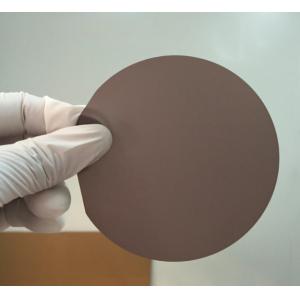
3inch dia76.2mm Lithium tantalate LiTaO3 lithium niobate LiNbO3 wafer substrates,
Black LT and LN wafer for saw,3inch, 4inch,6inch LiTaO3 wafer
Piezoelectric Crystal Lithium Tantalate LT LiTaO3 crystals
Lithium Tantalate (LT, LiTaO3) has unique properties, which as a material finds uses in Electro-Optical and Acousto-Optical applications. These can be : surface acoustic wave devices, bulk acoustic wave devices, piezo-electric transducers and piezoelectric sensors.The 36° and 42 ° cuts of Lithium Tantalate have shown widespread adoption for the telecommunications mobile phone handset market at frequencies from 800 to 2100 MHz. These orientations show an optimized bandwidth / insertion loss trade off in performance and are dominating the ever expanding mobile handset sales.
Specification
SAW grade
Orientation | 36°Y-cut±0.2° | 42°Y-cut±0.2° | X-cut±0.2° | |
| Diameter | 76.2±0.3mm, 100±0.3mm ,150±0.3mm | |||
| 1st OF Flat | 22±2mm,32±2mm,47.5±2mm perpendicular to X-axis±0.2° | 22±2mm,32±2mm,47.5±2mm perpendicular to 112°Y±0.2° | ||
| 2st OF Flat | 10±2mm CW270°from 1st OF | 10±2mm CW315°from 1st OF | 10±2mm CW315° Or 270°from 1st OF | |
| Thickness | 200~250±25um,300-350±25um,500±25um | |||
| Front surface | "+",Ra<1nm, | |||
| Back surface | GC#1000, GC#2000 Lapped | |||
| LTV | <1um,at5x5mm zone | |||
| BOW | ≤25um | |||
Opitcal Grade LiTaO3/LiNbO3 wafers
Orientations X-cut Z-cut
Diameter 76.2±0.3mm 76.2±0.3mm
Orientation Flat
(OF) perpendicular to X±0.2°
Thickness 0.2-5mm
Surface Quality double side polished S/D 20/10,40/20
TTV <15um
BOW <30um
Curie Temperature 605±2°
Edge beveling Edge rouding
Feature Piezoelectric Crystal LiTaO3 crystals
| Excellent photoelectric property |
| High Damage Threshold |
| High Curie Temperature |
Piezoelectric Crystal LiTaO3 crystals
| Specification | Conventional | High Precision |
| Materials | LiTaO3(LT) | LiTaO3(LT) |
| Orientation | X-112°Y,36°Y,42°Y±0.5° | X-112°Y,36°Y,42°Y±0.5° |
| Parallel | 30″ | 10'' |
| Perpendicular | 10′ | 5' |
| surface Quality | 40/20 | 20/10 |
| Wavefront Distortion | λ/4@632nm | λ/8@632nm |
| Surface Flatness | λ/4@632nm | λ/8@632nm |
| Clear Aperture | >90% | >90% |
| Chamfer | <0.2×45° | <0.2×45° |
| Thickness/Diameter Tolerance | ±0.1 mm | ±0.1 mm |
| Maximum dimensions | dia150×50mm | dia150×50mm |
| Properties | LiTaO3(LT) |
| Type of Material | Single Crystal |
| Crystal Structure | Trigonal,a = 5.154, c = 13.784Å |
| Melting Point | 1650℃ |
| Curie Temperature | 607℃ |
| Transmission Range | 400 – 5000 nm |
| Absorption edge | 270nm |
| Absorption loss | < 0.15 %/cm @ 1064 nm |
| Refractive Index | no=2.176,ne=2.180(at 0.633 µm) no=2.131,ne=2.134(at 1.2 µm) |
| Density | 7.45g/cm3 |
| Thermal Conductivity | 8.78x 10⁻⁷ m2/sec |
| Optical homogeneity | ~10-5 |
| Hardness (Mohs) | 5 |
| Elastic Coefficient | CE11 2.33(X 1011 N/m2) CE33 2.77(X 1011 N/m2) |
| Dielectric Constant | ε11/ε0 52.7 ε33/ε0 44.5 |
| Solubility in Water | insoluble in water |
| NLO Coefficients | d33 = 13.8 pm/V |
| d22= 2.4 pm/V | |
| d11= 0.85 pm/V | |
| Electro-Optic Coefficients | r31 =8.4 pm/V, @633nm |
| r22 =20 pm/V, @633nm | |
| r33 =30.5 pm/V, @633nm | |
| Damage Threshold | 2 MW/cm2@532nm |
| Standard Diameter | dia150x50mm |
FAQ
Q1. Is your company a factory or trade company?
We have a factory and we also do export by ourself trading company
.
We are the Sapphire substrates manufactuer and also can produce many type crystal into wafers.
Q2. Could you supply sample?
Yes,we can supply sample according to customer's requirement.
Q3. Do you have any stock of wafer or ingots?
We process many size wafer and lens according to customer
requirement.
almost 3inch ,4inch standard thickness wafers is in stock.
So we have few size in stock if it's commen specification.
Q4.Where is your company located?
Our company located in shanghai,China. factory is in wuxi city.
Q5. How long will take to get the products?
Generally it will take 1-3 weeks to process,standard wafer size
common can be deliveried in 2weeks
if customized size It is depend on the quantity and the size of the products.

Piezoelectric Crystal LiTaO3 LiNbO3 Wafers , Black LT And LN Wafer For Saw
Inquiry Cart
0