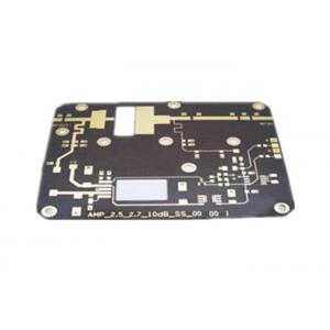
Rogers5880 4 Layer Base Station Black Soldermask Double Sided PCB
Brand Name:XCE
Certification:CE,ROHS, FCC,ISO9008,SGS,UL
Model Number:XCEM
Minimum Order Quantity:1pcs
Delivery Time:5-10 days
Payment Terms:T/T,Western union
Contact Now
Add to Cart
Site Member
Location:
Shenzhen Guangdong China
Address:
Room 403 Block A,Huafeng SOHO Creative World Hangcheng Industrial Zone Qianjin 2nd Road,Xixiang Baoan Shenzhen,China
Supplier`s last login times:
within 27 hours
Shipping
lt's easy to get a shipping quote! Just click the button below and complete the short form.
Get Shipping Quote
Product Details
Company Profile
Product Details
Rogers5880 Base Station Black Soldermask Double Sided PCB
Customize 2 layer Rogers5880 PCB board,this is black soldermask
finished surface microwave Rogers PCB,we can according to your
gerber file custom rogers printed circuit boards,not only have 2
layer rogers5880 board,we are also have multi-layer rogers
board,with Rogers4350 PCB,Rogers4003 PCB,rogers5880 PCB,Rogers3003
PCB,Rogers3010 PCB,Rogers6010 PCB and so on.
Rogers5880 Base Station Black Soldermask Double Sided PCB
Annual stock meterial:Rogers,Taconic,Arton,Isola,F4B
Layer No.1-16
Min board thickness:2 layer 0.2mm
4 layer 0.4mm
6 layer 0.6mm
8 layer 0.8mm
10 layer 1.0mm
Max panel size:508*610mm
Board thickness tolerance:T≥0.8mm±8%,T<0.8mm±5%
Wall hole copper thickness:>0.025mm(1mil)
Finished hole:0.2mm-6.3mm
Min line width:4mil/4mil(0.1/0.1mm)
Min bonding pad space:0.1mm(4mil)
PTH aperture tolerance:±0.075mm(3mil)
NPTH aperture tolerance:±0.05mm(2mil)
Hole site deviation:±0.05mm(2mil)
Profile tolerance:±0.10mm(4mil)
Board bend&warp:≤0.7%
Rogers5880 Base Station Black Soldermask Double Sided PCB
Electronic Rogers5880 circuits,most customers are customize and
order rogers5880 PCB,usually they will send gerber file to us
first,then tell us the quantity,board thickness,finished
surface,finished copper,color for soldermask or silkscreen,then we
will quote better price to them.Some Rogers will difficult,need
blind&buried hole,it will need some more time to quote that
RF and Antenna Design
Capabilities
Custom and Commercial Communication Systems
Complete Wireless System Architecture and Design
Miniature RF Design
Baseband Design
Wireless Firmware
Concept to Production
High and Low Volumes
| Seq | Item | capability |
| 1 | Base Material | FR-4, High TG FR-4 , Halogen Free material ,CEM-3,CEM-1,PTFE,Rogers ,Arlon ,Taconic,Aluminum base,Teflon,PI ,etc |
| 2 | Layers | 1-40 ( ≥30 layers needs review ) |
| 3 | Finished inner/outer copper thickness | 0.5-6OZ |
| 4 | Finished board thickness | 0.2-7.0mm(≤0.2mm needs review),≤0.4mm for HASL |
| Board thickness≤1.0mm: +/-0.1mm 1<Board thickness≤2.0mm: +/-10% Board thickness>2.0mm: +/-8% | ||
| 5 | Max panel size | ≤2sidesPCB: 600*1500mm Multilayer PCB: 500*1200mm |
| 6 | Min conductor line width/spacing | Inner layers: ≥3/3mil Outer layers: ≥3.5/3.5mil |
| 7 | Min hole size | Mechanical hole: 0.15mm Laser hole: 0.1mm |
| Drilling precision: first drilling First drilling: 1mil Second drilling: 4mil | ||
| 8 | Warpage | Board thickness≤0.79mm: β≤1.0% 0.80≤Board thickness≤2.4mm: β≤0.7% Board thickness≥2.5mm: β≤0.5% |
| 9 | Controlled Impedance | +/- 5 % Ω(<50Ω),+/-10%(≥50Ω),≥50Ω+/-5% (needs review) |
| 10 | Aspect Ratio | 15:01 |
| 11 | Min welding ring | 4mil |
| 12 | Min solder mask bridge | ≥0.08mm |
| 13 | Plugging vias capability | 0.2-0.8mm |
| 14 | Hole tolerance | PTH: +/-3mil NPTH: +/-2mil |
| 15 | Outline profile | Rout/ V-cut/ Bridge/ Stamp hole |
| 16 | Solder mask color | Green,yellow,black,blue,red,white,matte green |
| 17 | Component mark color | white,yellow,black |
| 18 | Surface treatment | OSP: 0.2-0.5um HASL: 2-40um Lead free HASL: 2-40um ENIG: Au 1-10U’’ ENEPIG: PB 2-5U’’/ Au 1-8U’’ Immersion Tin:0.8-1.5um Immersion silver: 0.1-1.2um Peelable blue mask Carbon ink Gold plating: Au 1-150U’’ |
| 19 | E-Test | Flying probe tester : 0.4-6.0mm,max 19.6*23.5inch |
| Min spacing from test pad to board edge : 0.5 mm | ||
| Min conductive resistance : 5 Ω | ||
| Max insulation resistance : 250 MΩ | ||
| Max test voltage : 500 V | ||
| Min test pad diameter : 6 mil | ||
| Min test pad to pad spacing : 10 mil | ||
| Max test current : 200 MA | ||
| 20 | AOI | Orbotech SK-75 AOI : 0.05-6.0mm,max 23.5*23.5inch |
| Orbotech Ves machine : 0.05-6.0mm,max 23.5*23.5inch | ||
Rogers5880 Base Station Black Soldermask Double Sided PCB
Rogers board Customized in different requirements and
quantity,price will have little difference,more quantity,unit price
will more cheaper for rogers5880 board.If Customize more quantity
for rogers5880 board,we can consider open test fixture,then for
reproduction order,will not charge test fee again,if just
sample,will charge engineer and test fee again
1. What is your minimum order quantity?
A. The MOQ is 1 PCS
2. What payment do you accept ?
A. T/T, Western Union, Paypal
3. What kind of PCB file format I need to submit for production?
A. Gerber files, BOM
4. No PCB file/Gbr file, only have the PCB sample,can you produce
it for me?
A. Send us the sample, and we will work out the gerber files and
clone the pcb for you.
5. Are my PCB files safe when I submit them to you for
manufacturing?
A:We respect customer's copyright and will never manufacture PCB
for someone else with your files unless we receive written
permission from you, nor will we share these files with any other
3rd parties. We can sign NDA with you.
6. How about the lead time?
A:Sample: 5 to 12working days
mass production: 7 to 18 working days
The lead time depends on your final confirmation of the quantity.
7. Which countries have you worked with?
A: We have built cooperation with customers from all over the
world, mostly North America and Europe

Rogers5880 4 Layer Base Station Black Soldermask Double Sided PCB
Inquiry Cart
0