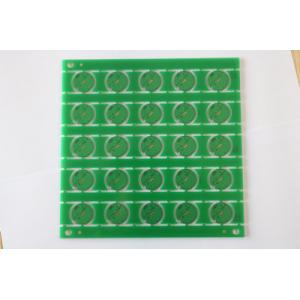
Multilayer Rigid PCB / Hiigh Density 8 Layer PCB PLC Power Circuit Board
Brand Name:XCE
Certification:CE,ROHS, FCC,ISO9008,SGS,UL
Model Number:XCEM
Minimum Order Quantity:1pcs
Delivery Time:5-10 days
Payment Terms:T/T,Western union
Contact Now
Add to Cart
Site Member
Location:
Shenzhen Guangdong China
Address:
Room 403 Block A,Huafeng SOHO Creative World Hangcheng Industrial Zone Qianjin 2nd Road,Xixiang Baoan Shenzhen,China
Supplier`s last login times:
within 27 hours
Shipping
lt's easy to get a shipping quote! Just click the button below and complete the short form.
Get Shipping Quote
Product Details
Company Profile
Product Details
Multilayer Rigid PCB/ Hiigh-Density 8-Layer PCB PLC Power Circuit Board
Quick detail:
| Origin:China | Special: FR4 Material |
| Layer:8 | Thickness:1.6mm |
| Surface: ENIG | Hole:0.5 |
Specification:
Electronic Scale PCB With 0.8mm Thickness 94V0 Electronic Board Green Soldermask White Silkscreen,
FR - 4 epoxy glass fiber cloth substrate, based on epoxy resin as binder, with electronic level glass fiber cloth as reinforcing material of substrate. Its bonding sheet and thin copper-clad r.p. panel and inner core is an important base material in production of multilayer printed circuit board,This kind of product is mainly used for double-sided PCB, dosage is very large. Epoxy glass fiber cloth substrate, the most widely used model for FR - 4, in recent years because of the electronic product installation technology and PCB technology development needs, appeared high Tg FR - 4 products.
BGA's full name Ball Grid Array (solder ball array package), which is in the bottom of the package substrate array solder ball as the circuit I / O terminals and printed circuit board (PCB) interconnection. The device using this technology is a surface mount device package.
PBG (Plastic Ball Grid Array), which uses BT resin / glass laminate as the substrate, plastic (epoxy molding compound) as the sealing material, solder ball can be divided into lead solder (63Sn37Pb, 62Sn36Pb2Ag) and lead-free solder Sn96.5Ag3Cu0.5), solder ball and package connections do not require additional use of solder.
Parameter:
| o | Item | Data |
| 1 | Layer: | 1 to 24 layers |
| 2 | Material type: | FR-4, CEM-1, CEM-3, High TG, FR4 Halogen Free, Rogers |
| 3 | Board thickness: | 0.20mm to 3.4mm |
| 4 | Copper thickness: | 0.5 OZ to 4 OZ |
| 5 | Copper thickness in hole: | >25.0 um (>1mil) |
| 6 | Max. Board Size: | (580mm×1200mm) |
| 7 | Min. Drilled Hole Size: | 4mil(0.1mm) |
| 8 | Min. Line Width: | 3mil (0.075mm) |
| 9 | Min. Line Spacing: | 3mil (0.075mm) |
| 10 | Surface finishing: | HASL / HASL lead free, HAL, Chemical tin, Chemical Gold, Immersion Silver/Gold, OSP, Gold plating |
| 11 | Solder Mask Color: | Green/Yellow/Black/White/Red/Blue |
| 12 | Shape tolerance: | ±0.13 |
| 13 | Hole tolerance: | PTH: ±0.076 NPTH: ±0.05 |
| 14 | Package: | Inner packing: Vacuum packing / Plastic bag,Outer packing: Standard carton packing |
| 15 | Certificate: | UL,SGS,ISO 9001:2008 |
| 16 | Special requirements: | Buried and blind vias+controlled impedance +BGA |
| 17 | Profiling: | Punching, Routing, V-CUT, Beveling |
| 1 | Layers | Single Sided,2 to 18 Layer |
| 2 | Board material type | FR4,Rogers,Taconic,F4B,Isola,Nelco and more |
| 3 | Compound material lamination | 4 to 6 layers |
| 4 | Maximum dimension | 610 x 1,100mm |
| 5 | Dimension tolerance | ±0.13mm |
| 6 | Board thickness coverage | 0.2 to 6.00mm |
| 7 | Board thickness tolerance | Board thickness≤1.0mm: +/-0.1mm 1<Board thickness≤2.0mm: +/-10% Board thickness>2.0mm: +/-8% |
| 8 | DK thickness | 0.076 to 6.00mm |
| 9 | Minimum line width | 0.10mm |
| 10 | Minimum line space | 0.10mm |
| 11 | Outer layer copper thickness | 8.75 to 175µm |
| 12 | Inner layer copper thickness | 17.5 to 175µm |
| 13 | Drilling hole diameter (mechanical drill) | 0.25 to 6.00mm |
| 14 | Finished hole diameter (mechanical drill) | 0.20 to 6.00mm |
| 15 | Hole diameter tolerance (mechanical drill) | 0.05mm |
| 16 | Hole position tolerance (mechanical drill) | 0.075mm |
| 17 | Laser drill hole size | 0.10mm |
| 18 | Board thickness and hole diameter ratio | 10:01 |
| 19 | Solder mask type | Green, Yellow, Black, Purple, Blue, White and Red |
| 20 | Minimum solder mask | Ø0.10mm |
| 21 | Minimum size of solder mask separation ring | 0.05mm |
| 22 | Solder mask oil plug hole diameter | 0.25 to 0.60mm |
| 23 | Impedance control tolerance | ±10% |
| 24 | Surface finish | Hot air level, ENIG, immersion silver, gold plating, immersion tin and gold finger |
| 25 | Certificate | ROHS, ISO9001:2008, SGS, UL certificate |
| 26 | Acceptable file format | Gerber file,PROTEL series,PADS series,POWER PCB series,AutoCAD |

Multilayer Rigid PCB / Hiigh Density 8 Layer PCB PLC Power Circuit Board
Inquiry Cart
0