Custom PCB Circuit Boards For Wireless 5G Mobile Communication Devices
Brand Name:XCE
Certification:CE,FCC,UL,SGS
Model Number:XCER
Minimum Order Quantity:1 pcs
Delivery Time:3-8 days
Place of Origin:China
Contact Now
Add to Cart
Site Member
Location:
Shenzhen Guangdong China
Address:
Room 403 Block A,Huafeng SOHO Creative World Hangcheng Industrial Zone Qianjin 2nd Road,Xixiang Baoan Shenzhen,China
Supplier`s last login times:
within 27 hours
Shipping
lt's easy to get a shipping quote! Just click the button below and complete the short form.
Get Shipping Quote
Product Details
Company Profile
Product Details
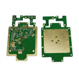
Risho Material Custom PCB Circuit Boards For Wireless 5G Mobile
Communication Devices
Quick Details
Model Number: XCER
Number of Layers: 2-Layer
Base Material: Risho
Copper Thickness: Inner 1/2 oz-4oz;Outer 1oz-5oz
Board Thickness: 0.8mm
Min. Hole Size: 0.2mm-6.3mm
Min. Line Width: 3MIL
Min. Line Spacing: 3mil
Surface Finishing: Immersion
Color: Green
Service: One-stop Service
Certificate: ISO9001,SGS,UL
Name: High frequency pcb
Testing Service: standard
Type: Panel
Shipping: Buyer's Requirement
PCB Introduction
1, Surface finish: Immersion Gold/HALS/OSP/Gold finger/Carbon print/Peelable mask/Blue mask/Plating gold
2, Solder mask colour: green/white/yellow/blue/red/black
3, Silk screen: white/black/yellow/red/blue/green
4, Applied in industrial facilities/medical facilities/consumer electronics/telecommunications/power supply
Technology parameter:
Layer | 2 layer |
Material type | Risho |
Board thickness | 0.8mm |
Copper thickness | 0.5OZ |
Copper thickness in hole | >25.0 um (>1mil) |
| Max. Board Size: 23 × 25 (580mm×900mm) |
Min. Drilled Hole Size: 3mil (0.075mm) | |
Min. Line Width: 3mil (0.075mm) | |
Min. Line Spacing: 3mil (0.075mm) | |
| HASL / HASL lead free, HAL, Chemical tin, Chemical Gold, Immersion Silver/Gold, OSP, Gold plating |
| Shape tolerance: ±0.13 |
Hole tolerance: PTH: ±0.076 NPTH: ±0.05 | |
Certificate | UL, ISO 9001, ISO 14001 |
Special requirements | Buried and blind vias+controlled impedance +BGA |
Profiling | Punching, Routing, V-CUT, Beveling |
| Any other special material please feel free to let us know | |
PCB Technical Specification
Number of Layer 1,2,4 or 6,upto 24 layer
Order Quantity 1 to 50,0000
Board Shape Retangular,round,slots,cutouts,complex,irregular
Board Type Rigid, Flexible, Rigid-flexible
Board Material FR-4 glass epoxy, FR-4 high Tg, Rohs
compliant,Aluminum,Rogers,etc.
Board Cutting Shear,V-score,Tab-routed
Board Thickness 0.2-4.0mm, Flex 0.01-0.25mm
Copper Weight 1.0, 1.5, 2.0 oz
Solder Mask Double-sided green LPI,Also support
Red,White,Yellow,Blue,Black
Silk Screen Double-sided or single-sided in white,yellow,black,or
negative
Silk Screen Min Line Width 0.006'' or 0.15mm
Max Board Dimensions 20 inch*20inch or 500mm*500mm
Min Trace/Gap 0.10mm, or 3mils
Min Drill Hole Diameter 0.01'',0.25mm, or 10mils
Surface Finish HASL,Nickle,Immersion Gold,Immersion Tin,Immersion
Silver,OSP,etc.
Board Thickness Tolerance ±10%
Copper Weight Tolerance ± 0.25 oz
Minimal Slot Width 0.12'', 3.0mm, or 120mils
V-Score Depth 20-25% of board thickness
Design File Formate Gerber RS-274,274D,Eagle and AutoCAD's DXF,DWG

Custom PCB Circuit Boards For Wireless 5G Mobile Communication Devices
Inquiry Cart
0