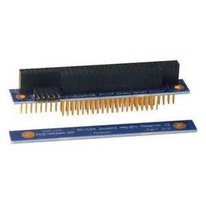
ENIG , HASL flash drive circuit prototype pcb circuit boards 3 mil Min. Line
Brand Name:WonDa
Certification:CE, ROHS, UL
Minimum Order Quantity:None
Delivery Time:5-15 days
Payment Terms:T/T, W.U, L/C
Place of Origin:Shenzhen, China
Contact Now
Add to Cart
Active Member
Location:
Shenzhen Guangdong China
Address:
703, Yufeng building,7-9# Jinhai road, Yantian community,Xixiang street,Bao'an district, Shenzhen city
Supplier`s last login times:
within 3 hours
Shipping
lt's easy to get a shipping quote! Just click the button below and complete the short form.
Get Shipping Quote
Product Details
Company Profile
Product Details
ENIG , HASL flash drive circuit prototype pcb circuit boards 3 mil Min. Line
Specifications
Manufacture flash drive circuit pcb board,pcb prototype1.High quality circuit board
2.quick turn
3.Strong engineering suppor
Manufacture automatic gate pcb board,pcb prototype
Detail:
(1)PCB and PCBA
(2)PCB Copy
(3)UL,ISO,RoHS,SGS,IPC
(4)PCB manufacturer
(5)Small order accepted
(6)high quality and resonable price
- specialized in single-sided PCB, double-sided PCB, multilayer PCB and PCBA.
- Material Type: FR4,CEM-1,non-halogen,Aluminium, high frequency, 94-V0, PI, High TG
- Surface treatment: HASL, LF, Immersion Gold, Immersion Tin/ silver, Gold Finger, OSP
Specification:
Item | Capabilities | |||
1.Base Material | FR-4 / High TG FR-4 / Lead free Materials (ROHS Compliant) / Halogen Free material /CEM-3/CEM-1/ /PTFE/ROGERS/ARLON/TACONIC | |||
2.Layers | 1-30 | |||
3.Finised inner/outer copper thickness | 1-12OZ | |||
4.Finished board thickness | 0.2-7.0mm | |||
Tolerance | Board thickness≤1.0mm: +/-0.1mm 1<Board thickness≤2.0mm: +/-10% Board thickness>2.0mm: +/-8% | |||
5.Max panel size | ≤2sidesPCB: 600*1500mm Multilayer PCB: 500*1200mm | |||
6.Min conductor line width/spacing | Inner layers: ≥3/3mil Outer layers: ≥3.5/3.5mil | |||
7.Min hole size | Mechanical hole: 0.15mm Laser hole: 0.1mm | |||
Drilling precision: first drilling | First drilling: 1mil Second drilling: 4mil | |||
8.Warpage | Board thickness≤0.79mm: β≤1.0% 0.80≤Board thickness≤2.4mm: β≤0.7% Board thickness≥2.5mm: β≤0.5% | |||
9.Controlled Impedance | +/-5% | |||
10. Aspect Ratio | 15:1 | |||
11.Min welding ring | 4mil | |||
12.Min solder mask bridge | ≥0.08mm | |||
13.Plugging vias capability | 0.2-0.8mm | |||
14. Hole tolerance | PTH: +/-3mil NPTH: +/-2mil | |||
15.Outline profile | Rout/ V-cut/ Bridge/ Stamp hole | |||
16.Surface treatment | OSP: 0.5-0.5um HASL: 2-40um Lead free HASL: 2-40um ENIG: Au 1-10U’’ ENEPIG: PB 2-5U’’/ Au 1-8U’’ Immersion Tin:0.8-1.2um Immersion silver: 0.1-1.2um Peelable blue mask Carbon ink Gold plating: Au 1-150U’’ | |||
17. E-testing pass percent | 97% pass for the first time,+/-2%(tolerance) | |||
FQC-Physical Lab: Reliability tests | ||||
18.Certificate | ROHS UL:E327776 ISO9001:2008 IPC SGS | |||
Our equipments | ||||
1.Drilling workshop | 4 drilling bits of drilling machine: 4 sets 2 drilling bits of drilling machine: 2 sets | |||
2. photo plotting workshop | Israel “ORBOTECH” Photo Plotters | |||
3.AOI | AOI machine | |||
4.IPQC | “OXFORD” CMI 700 Copper Thickness Tester | |||
5.Impedance test | USA “Tektronix” DSA 8200 Impedance Tester | |||
6.Outline workshop | CNC routing machine: 7 sets angle-cutting machine V-cut machine | |||
7.Testing Workshop | Surpass X-600: 2sets WTD FT-2808: 5sets WTD HV300: 1set | |||
8.X-ray | X-ray machine | |||
Acceptable file format | ||||
GERBER file, PROTEL series, PADS series, POWER PCB series, AutoCAD series. | ||||

ENIG , HASL flash drive circuit prototype pcb circuit boards 3 mil Min. Line
Inquiry Cart
0