semiconductor FCCSP Package Substrate manufacture
Brand Name:Horexs
Certification:UL
Minimum Order Quantity:1 square meter
Delivery Time:7-10 working days
Payment Terms:L/C, D/P, T/T, Western Union, MoneyGram
Place of Origin:china
Contact Now
Add to Cart
Verified Supplier
Location:
Shenzhen China
Address:
Tianyue building 711,518100 shajing centre bao'an district Shenzhen city
Supplier`s last login times:
within 32 hours
Shipping
lt's easy to get a shipping quote! Just click the button below and complete the short form.
Get Shipping Quote
Product Details
Company Profile
Product Details
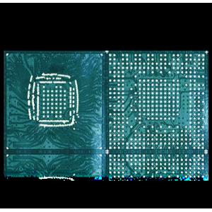
Application:FCCSP package,IC assembly,Semiconductor package,IC package,Consumer electronics,Computer,others;
Spec.of Substrate production:
Mini.Line space/width:1mil (25um)
Finished thickness:0.3mm;
Material brand:Mainly brand:SHENGYI,Mitsubishi(BT-FR4),mitsuiseiki,OhmegaPly,Ticer,AMC,Isola,AGC,Neclo,Rogers,Taconic,Others;
Surface finished:Mainly immersion gold,support customize such as OSP/Immersion silver,tin,more;
Copper:10-15um or Customize;
Layer:1-6 layer (Customize);
Soldermask:Green or Customize (Brand:Soldermask:TAIYO INK,ABQ)
Short introduction of Horexs Manufacturer:
HOREXS-Hubei is belong to HOREXS Group, is one of the leading and fast-growing Chinese IC substrate manufacturer.Which was located in Huangshi city of Hubei province China. Factory-Hubei is more than 60000 square meters floor space, which invested more than 300 million USD. IC Substrate Capacity 600,000SQM/Year,Tenting&SAP process. HOREXS-Hubei is committed to the development of IC substrate in China, striving to become one of the top three IC substrate manufacturers in China, and striving to become a world-class IC board manufacturer in the world . Technology like L/S 20/20un,10/10um.BT+ABF materials. Support: Wire bonding Substrate Wire bonding(BGA) Substrate Embedded (Memor y IC substrate) MEMS/CMOS,Module(RF,Wireless ,Bluetooth) 2/4/6L (1+2+1/2+2+2/1+4+1),Buildup(Buried/Blind hole) Flipchip CSP; Others ultra ic package substrate.
When you send inquiry us,Pls be know that we have to get the following :
1-Substrate production sepc. information;
2-Gerber files(Substrate designer/engineer can export it from your layout software,also send us drilling file)
3-Quantity request,Including sample;
4-Multilayer Substrate,please also provide us layer stack-up/Buildup information;
Process Capability
Our Technology
• Fine pattern by MSAP(20/20um) and Tenting(30/30um)
• Various Applicable Technical Option
- Thin Core Technology
- All type Surface Finish
- SR Flatness Process, Build up / Via Filling Tech.
- Tailless, Etch-back Process
- Fine Pitch SOP process
• High Quality and Reliability Substrate
• High Speed Delivery : No need film, No outsourcing
• Competitive Low Running Cost
Shipping supporting:
DHL/UPS/Fedex;
By air;
Customize express(DHL/UPS/Fedex)


semiconductor FCCSP Package Substrate manufacture
Inquiry Cart
0