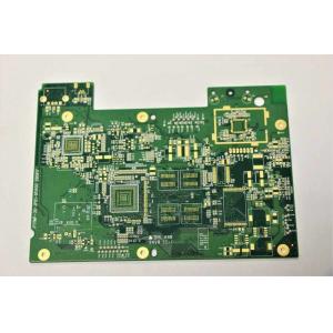
Multilayer PCB with High Frequency Layout Design Blind Buried vias pcb
Brand Name:found
Certification:ISO UL
Model Number:fd21
Minimum Order Quantity:1
Payment Terms:T/T
Place of Origin:China
Contact Now
Add to Cart
Active Member
Location:
Shenzhen Guangdong China
Address:
NO.1 Industry Park, XinSheng Village, Longgang District, ShenZhen
Supplier`s last login times:
within 1 hours
Shipping
lt's easy to get a shipping quote! Just click the button below and complete the short form.
Get Shipping Quote
Product Details
Company Profile
Product Details
AddThis Sharing Buttons
Share to FacebookFacebookShare to TwitterTwitterShare to
LinkedInLinkedInShare to PinterestPinterestShare to ...AddThis
Multilayer PCB with High Frequency Layout Design Blind Buried vias pcb
- Product Description 1.1 General description This is a type of high frequency PCB built on 10mil RO4350B substrate with Tg 280°C for the application of portable antenna. It's 0.3 mm thick with 2 layers copper, black silkscreen directly on substrate and immersion gold on pads. The base...
Chat Now
- Product Details
Product Description
1.1 General description
This is a type of high frequency PCB built on 10mil RO4350B
substrate with Tg 280°C for the
application of portable antenna. It's 0.3 mm thick with 2 layers
copper, black silkscreen directly
on substrate and immersion gold on pads. The base material is from
Rogers Corp supplying
4 types PCBs per panel. They're fabricated per IPC 6012 Class 2
using supplied Gerber data.
Each 50 panels are packed for shipment.
1.2 Features and benifits
a. RO4350B exhibits a stable dielectric constant over a broad
frequency range. This makes it
an ideal substrate for broadband applications;
b. Excellent high frequency performance due to low dielectric
tolerance and loss;
c. Tg > 280 C;
d. 16000 square meter workshop;
e. 30000 square meter month capability;
f. RoHS materials;
g. Eligible products rate of first production: >95%
h. No quality complaint is meant to save money;
i. No MOQ, low cost for prototypes and small runs quantity.
1.3 Application
LNA, Photocoupler, RFID, Trunk amplifier
Hot Tags: high frequency multilayer pcb layout design blind vias,
China, factory, manufacturers, suppliers, quotation, made in China
Edge Platting PCB matt green PCB
4-Layer High Frenquency Rogers PCB
High Power Led bulb Pcb Immer gold
Fast Flex Carbon Board PCB
Rigid-Flex PCB Fast-Turn Prototype And Mass Poduction
3D Printer Controller Pcb Ims Leiterplatten Lamp Thi...
- Feedback
Your Name: | |
*E-mail: | |
Phone: | |
Company: | |
Title: | |
*Content: | |
Send |


Multilayer PCB with High Frequency Layout Design Blind Buried vias pcb
Inquiry Cart
0