Data Acquisition Motherboard Printed Circuit Board Custom Circuit Board Printing
Brand Name:FASTPCB
Minimum Order Quantity:10PCS
Payment Terms:L/C, T/T
Place of Origin:CHINA
Price:USD 0.01-100/PCS
Supply Ability:25,000 ㎡ / month Or 10PCS/48Hour(Double-Sided Printed Board)Or 10PCS/72Hour(Multilayer printed circuit board )
Contact Now
Add to Cart
Active Member
Location:
Shenzhen Guangdong China
Address:
Building B, Shangxing West Industrial Zone, No. 1001, West Ring Road, Shajing street, Bao'an District, Shenzhen, Guangdong, China
Supplier`s last login times:
within 23 hours
Shipping
lt's easy to get a shipping quote! Just click the button below and complete the short form.
Get Shipping Quote
Product Details
Company Profile
Product Details
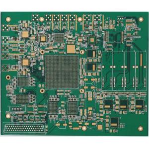
Data Acquisition Motherboard Printed Circuit Board
The Data Acquisition Motherboard Printed Circuit Board is the rigidity PCB circuit board developed and produced by Shenzhen Quanhong Electronics Co., Ltd. the HDI board is made of FR-4 material, surface gold deposition and laser drilling. The minimum line width and line spacing can reach 75um and the minimum hole diameter can reach 0.1mm. The buried blind hole circuit board is widely used in digital cameras, notebooks, mobile phones and other electronic products and automotive electronics.
HLC Process capability
| Item | HLC Advanced Technology | |||
| 2019 | 2020 | 2021 | ||
| Max Panel Width (inch) | 25 | 25 | 25 | |
| Max Panel Length (inch) | 29 | 29 | 29 | |
| Max Layer Count (L) | 16 | 18 | 36 | |
| Max Board thickness (mm) | 3.2 | 4 | 6 | |
| Max Board thickness Tolerance | +/-10% | +/-10% | +/-10% | |
| Base copper Thickness | Inner layer ( OZ ) | 4 | 6 | 8 |
| Outer Layer ( OZ ) | 2 | 3 | 4 | |
| Min DHS ( mm ) | 0.2 | 0.15 | 0.15 | |
| PTH Size Tolerance ( mil ) | +/-2 | +/-2 | +/-2 | |
| Back Drill (stub)( mil ) | ~ 3 | ~ 2.4 | ~ 2 | |
| Max. AR | 12:1 | 16:1 | 20:1 | |
| Item | HLC Advanced Technology | |||
| 2019 | 2020 | 2021 | ||
| M-drill tolerance | Inner layer ( mil ) | DHS + 10 | DHS + 10 | DHS + 8 |
| Outer Layer ( mil ) | DHS + 8 | DHS + 8 | DHS + 6 | |
| Solder mask Registration (um) | +/- 40 | +/- 30 | +/- 25 | |
| Impedance control | ≥50ohms | +/-10% | +/-10% | -/-8% |
| <50ohms | 5 Ω | 5 Ω | 4 Ω | |
| Min LW/S (Inner)@1oz base Cu ( mil ) | 3.0 / 3.0 | 2.6 / 2.6 | 2.5 / 2.5 | |
| Min LW/S (Outer)@1oz Cu ( mil ) | 3.5 / 3.5 | 3.0 / 3.5 | 3.0 / 3.0 | |
| Max dimple for POFV ( um ) | 30 | 20 | 15 | |
| Surface Finishing | ENIG, Immersion Ag, OSP, HASL, Immersion Tin, Hard Au | |||
HDI Process capability
| Item | HDI Advanced Technology | |||
| 2019 | 2020 | 2021 | ||
| Structure | 5+n+5 | 6+n+6 | 7+n+7 | |
| HDI Stack Via | AnyLayer(12L) | AnyLayer(14L) | AnyLayer(16L) | |
| Board Thickness(mm) | Min. 8L | 0.45 | 0.4 | 0.35 |
| Min. 10L | 0.55 | 0.45 | 0.4 | |
| Min. 12L | 0.65 | 0.6 | 0.55 | |
| MAX. | 2.4 | |||
| Min. Core Thickness ( um ) | 50 | 40 | 40 | |
| Min. PP Thickness ( um ) | 30(#1027PP) | 25(#1017PP) | 20(#1010PP) | |
| Base Copper Thickness | Inner Layer ( OZ) | 1/3 ~ 2 | 1/3 ~ 2 | 1/3 ~ 2 |
| Outer Layer ( OZ ) | 1/3 ~ 1 | 1/3 ~ 1 | 1/3 ~ 1 | |
| Item | HDI Advanced Technology | |||
| 2019 | 2020 | 2021 | ||
| Min. Mechanical Drill hole size(um) ** | 200 | 200 | 150 | |
| Max. Through Hole Aspect Ratio * | 8:1 | 10:1 | 10:1 | |
| Min. Laser via/Pad Size ( um ) | 75/200 | 70/170 | 60/150 | |
| Max. Laser Via Aspect Ratio | 0.8:1 | 0.8:1 | 0.8:1 | |
| Laser Via on PTH(VOP)design | Yes | Yes | Yes | |
| Laser X type through hole(DT≤200um) | NA | 60~100um | 60~100um | |
| Min. LW/S (L/S/Cu, um) | Inner Layer | 45 /45 /15 | 40/ 40/ 15 | 30/ 30 /15 |
| outer Layer | 50 /50/ 20 | 40 /50 /20 | 40 /40 /17 | |
| Min BGA Pitch (mm) | 0.35 | 0.3 | 0.3 | |
| Item | HDI Advanced Technology | |||
| 2019 | 2020 | 2021 | ||
| Solder mask Registration (um) | +/- 30 | +/- 25 | +/- 20 | |
| Min. Solder Mask Dam (mm) | 0.07 | 0.06 | 0.05 | |
| PCB Warpage Control | >= 50ohm | +/-10% | +/-8% | +/- 5% |
| < 50ohm | +/- 5ohm | +/- 3ohm | +/- 3ohm | |
| PCB Warpage Control | ≤0.5% | ≤0.5% | ≤0.5% | |
| cavity Depth accuracy (um) | Mechanical | +/- 75 | +/- 75 | +/- 50 |
| Laser directly | +/- 50 | +/- 50 | +/- 50 | |
| Surface Finishing | OSP,ENIG,Immersion Tin,Hard Au, Immersion Ag | OSP,ENIG,Immersion Tin,Hard Au,Immersion Ag, ENEPIG | ||
| Packaging & Delivery | |||||
| Packaging Details: | Inner: vacuum packing or Anti-static package, Outer: export carton or according to the customer's requirement. | ||||
| Port: | Shenzhen or Hongkong | ||||
| Lead Time: | Quantity(Pieces) | 1-10 | 11-100 | 101-1000 | >1000 |
| Est. Time(days) | 3-5 | 3-5 | 7-9 | To be negotiated | |
FAQ:
Q: What service do you have?
FASTPCB: We provide turnkey solution including PCB fabrication,
SMT, plastic injection & metal,final assembly, testing and
other value-added service.
Q: What is needed for PCB & PCBA quotation?
FASTPCB: For PCB: Quantity, Gerber file and technic
requirements(material,size, surface finish treatment, copper
thickness,board thickness).
For PCB: PCB information, BOM,Testing documents.
Q: How to keep our product information and design file secret ?
FASTPCB: We are willing to sign a NDA effect by customers side
local law and promising tokeep customers data in high confidential
level.
Q: What are the main products of your PCB/PCBA services?
FASTPCB: Automotive, Medical, Industry Control, IOT, Smart Home,
Military, Aerospace.
Q: What is your minimum order quantity (MOQ)?
FASTPCB: Our MOQ is 1 PCS, sample and mass production all can
support.
Q: Are you factory?
FASTPCB:Shangxing West Industrial Zone, Xihuan Road, Shajing Street, Bao 'an District, Shenzhen, Guangdong province, China

Data Acquisition Motherboard Printed Circuit Board Custom Circuit Board Printing
Inquiry Cart
0