Rigid Flexible 6OZ HASL FR4 HDI PCB Circuit Board
Brand Name:FASTPCBA
Certification:ISO9001, ISO14001, ISO13485, IATF16949
Model Number:Pcb Manufacturer
Minimum Order Quantity:1PCS
Payment Terms:L/C, D/A, D/P, T/T, Western Union, MoneyGram
Place of Origin:China
Contact Now
Add to Cart
Verified Supplier
Location:
Shenzhen Guangdong China
Address:
Shenzhen Guangming yulv Village Road Jade Spring beauty industrial district 18-1 building
Supplier`s last login times:
within 27 hours
Shipping
lt's easy to get a shipping quote! Just click the button below and complete the short form.
Get Shipping Quote
Product Details
Company Profile
Product Details
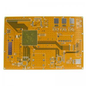
Shenzhen Professional Manufacturer Electronic Printing Circuit Board Pcb Maker HDI PCB Circuit Board
HDI Circuit Board
HDI is the abbreviation of High Density Interconnector. It is a
(technology) for the production of printed circuit boards. It uses
micro-blind and buried via technology for a circuit board with a
relatively high line distribution density. HDI is a compact product
designed for small-capacity users. It adopts modular design that
can be connected in parallel. One module has a capacity of 1000VA
(1U height) and is naturally cooled. It can be directly placed in a
19" rack, and up to 6 modules can be connected in parallel. The
product adopts full digital signal processing (DSP) technology and
multiple Patented technology, with full range of adaptable load
capacity and strong short-term overload capacity, regardless of
load power factor and crest factor.
PCB Capacities and Technical Specification
PCBA Capabilities
HDI Circuit Board Application
While electronic design continues to improve the performance of the
whole machine, it is also working hard to reduce its size. In small
portable products ranging from mobile phones to smart weapons,
"small" is an eternal pursuit. High-density integration (HDI)
technology can make terminal product designs more compact, while
meeting higher standards of electronic performance and efficiency.
HDI is widely used in mobile phones, digital (camcorder) cameras,
MP3, MP4, notebook computers, automotive electronics and other
digital products, among which mobile phones are the most widely
used. HDI boards are generally manufactured by the build-up method.
The more build-up times, the higher the technical grade of the
board. Ordinary HDI boards are basically one-time build-up.
High-end HDI uses two-time or more build-up technology. At the same
time, advanced PCB technologies such as stacking holes,
electroplating and filling holes, and laser direct drilling are
used. High-end HDI boards are mainly used in 3G mobile phones,
advanced digital cameras, IC carrier boards, etc.


Rigid Flexible 6OZ HASL FR4 HDI PCB Circuit Board
Inquiry Cart
0