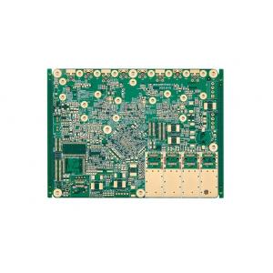
0.25MM Immersion Gold High Frequency PCB Design 12 Layer PCB Board 4 Mil
Brand Name:Global Success Circuits Co.,Ltd
Certification:UL(E324220) TS16949 ISO 9001
Model Number:GSC-P1A3DE
Minimum Order Quantity:1 Piece
Delivery Time:5 - 15 days
Payment Terms:T/T, D/P, D/A, L/C, Western Union
Contact Now
Add to Cart
Active Member
Location:
Shenzhen Guangdong China
Address:
Headquarters :F12, Xingji Building Shangxing Road Shajing Town ,Baoan District Shenzhen China
Supplier`s last login times:
within 1 hours
Shipping
lt's easy to get a shipping quote! Just click the button below and complete the short form.
Get Shipping Quote
Product Details
Company Profile
Product Details
0.25MM Immersion Gold High Frequency PCB Design 12 Layer PCB Board 4 Mil
Here at Global Succes, Standard PCB service refers to full feature printed circuit board manufacturing service. With 13 years' experience in PCB fabrication, we have handled hundreds of thousands of PCB projects, and covered almost all kinds of substrate material including Standard FR4, Aluminum, Rogers, etc. This page only touches standard FR4 based PCB. For PCBs with special technical substrate, please kindly refer to corresponding webpage for information.
Unlike Prototype PCB service, our Standard PCB service has tighter production tolerances.
If you have any question or concern on our Custom PCB capabilities or your demanded custom circuit spec is not included in the above table, please feel free to contact us.We're always available for you.
It is recommended to use Standard PCB service when your design is ready to transform from prototype phase to production phase. We can manufacture up to 10 million pieces high quality PCBs with very competitive prices. To endow your project with expected function and more possibilities, we offer advanced features for Standard PCB services. Comprehensive capabilities can be found in the following table:
PCB manufacturing capability - Item | Production | Prototype |
Max Layer Count | 2-14 Layers | 2-16 Layers |
Max Board Thickness | 0.175” | 0.200” |
Max Board Size | 26"×26") | 26"×26") |
Min Board Thickness | 0.014” | 0.012” |
Min Track Width/Gap, Outer/Inner (17 micron) | 0.003” / 0.003” | 0.003” / 0.003” |
Min Hole Size | 0.006” | 0.006” |
Min Annular Ring (outer layer) | 0.003” | 0.003” |
Min Annular Ring (inner layer) | 0.004” | 0.004” |
Drill to Metal | 0.008” | 0.007” |
Drilling Tolerance(PTH&NPTH) | +/- 0.002” | +/- 0.002” |
Hole Position Tolerance | +/- 0.003” | +/- 0.002” |
Min Solder mask Registration | 0.001” | 0.001” |
Board Thickness(<1.0mm) Tolerance | +/-0.004" | +/-0.004" |
Board Thickness(>1.0mm) Tolerance | +/-10% | +/-10% |
Inner Layer Registration | +/- 0.004” | +/- 0.004” |
Outline Routed Tolerance | +/- 0.004” | +/- 0.004” |
Outline Scored Tolerance | +/- 0.008” | +/- 0.008” |
Aspect Ratio | </= 8:1 | </= 12:1 |
Min QFP Pitch (not HASL) | 0.016” | 0.010” |
Controlled Impedance(Single ended) | 50 - 90 ohms +/- 6% | 50 - 90 ohms +/- 7% |
Max Internal Copper Wt. | 6 oz | 7 oz |
HDI(1+N+1 Max Layer Count)-Min Via Size | 0.004” | 0.004” |
Surface Finish Selection: | ||
Surface finish treatment | Production | Prototype |
Liquid Photo-Imageable Solder Mask (LPI) | 10-40um | 10-40um |
Peelable Solder Mask | 0.2-0.5mm | 0.2-0.5mm |
Conductive Carbon Ink | ≤20Ω | ≤20Ω |
Hot Air Solder Leveled Finish (HASL) /HAL Lead Free | 1-30um | 1-30um |
Organic Solderability Preservatives(OSP) | Entek Cu 106A HT , Preflux F2 LX | Entek Cu 106A HT, Preflux F2 LX |
Electroless Immersion Gold | Ni: 2.0-10um Au: 0.025-0.10um | Ni: 2.0-10um Au: 0.025-0.10um |
Electrolytic Flash Gold | Ni: 2.5-10um Au: 0.020-0.075um | Ni: 2.5-10um Au: 0.020-0.075um |
Electroless Immersion Silver | 0.10-0.5um | 0.10-0.5um |
Electroless Immersion Tin | 0.3-2.0um | 0.3-2.0um |
Gold tab/finger plating(3u"-60u") | Ni: 2.5-10um Au: 0.25-1.50um | Ni: 2.5-10um Au: 0.25-1.50um |
Selective Surface Treatment | ENIG+OSP, ENIG+G/F, Flash Gold+HAL, Flash Gold+G/F,Immersion Silver+G/F, Immersion Tin+G/F | |
Special Materials Selection: | ||
High Performance Materials | Production | Prototype |
Al / Cu Substrate | Yes | Yes |
Bismalemide Triazine | Yes | Yes |
Nelco N 4000 - 13 | Yes | Yes |
Nelco N 4000 - 13 (SI) | Yes | Yes |
Nelco N 4000 - 12 | Yes | Yes |
Rogers RO4350 | Yes | Yes |
Rogers RO4003 | Yes | Yes |
Rogers RO4233 | Yes | Yes |
Taconic RF-35 | Yes | Yes |
Taconic RF-45 | Yes | Yes |
Taconic TLX-8 | Yes | Yes |
Arlon AD250 | Yes | Yes |
Arlon AD320 | Yes | Yes |
Arlon IsoClad917 | Yes | Yes |
Isola FR408 | Yes | Yes |
Isola 370HR | Yes | Yes |
Isola 406HR | Yes | Yes |
Getek / Megtron | Yes | Yes |
Polyclad PCL-FR370HR | Yes | Yes |
Hitachi MCL-BE-67G | Yes | Yes |
Halogen Free | Yes | Yes |
Other Normal Materials: | ||
Normal Material | Production | Prototype |
Solder Mask Material | Taiyo or Tumura | Taiyo or Tumura |
Laminate Material | Shengyi ITEQ (IT140,IT150,IT-140G,ANTI-CAF,IT155G,IT180) Nanya , Goword (GW40,GW4011 KB (KB-7150CEM,KB-6167,KB-6165,KB-6162,KB-6160/6160C,KB6165/6160) | Shengyi ITEQ (IT140,IT150,IT-140G,ANTI-CAF,IT155G,IT180) Nanya , Goword (GW40,GW4011 KB (KB-7150CEM,KB-6167,KB-6165,KB-6162,KB-6160/6160C,KB6165/6160) |
HASL Lead Free | SN100C | SN100C |
Peelable Mask | SD2955 | SD2955 |
PCB manufacturing Lead Time: | ||
Layer Count | Quick-turn Prototype | Mass Production |
2 Layers | 24 Hours | 12 Working Days |
4 Layers | 48 Hours | 13 Working Days |
6 Layers | 72 Hours | 14 Working Days |
8 Layers | 96 Hours | 14 Working Days |
10 Layers | 140 Hours | 16 Working Days |
12 Layers | 160 Hours | 17 Working Days |
14 Layers | 180 Hours | 20 Working Days |
16-20 Layers | Specified case by case | |
More than 20 Layers | Specified case by case | |


0.25MM Immersion Gold High Frequency PCB Design 12 Layer PCB Board 4 Mil
Inquiry Cart
0