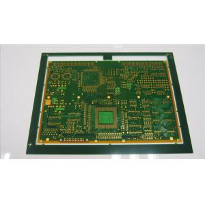
Industrial Equipment Multilayer PCB Board FR4 TG150 1Oz With Impedance Control
Brand Name:Global Success Circuits Co.,Ltd
Certification:ISO 9001:2015 UL , ISO 14001, TS16949
Model Number:GSC-L2M053
Minimum Order Quantity:1 Piece
Delivery Time:3 - 12 days
Payment Terms:L/C, D/P, T/T, Western Union
Contact Now
Add to Cart
Active Member
Location:
Shenzhen Guangdong China
Address:
Headquarters :F12, Xingji Building Shangxing Road Shajing Town ,Baoan District Shenzhen China
Supplier`s last login times:
within 1 hours
Shipping
lt's easy to get a shipping quote! Just click the button below and complete the short form.
Get Shipping Quote
Product Details
Company Profile
Product Details
Industrial Equipment Multilayer PCB Board FR4 TG150 1Oz With Impedance Control
Manufacturing Multilayer PCBs (Up to 14 Layers)
The demand for multilayer boards has been on the rise. The drive for electronics to be smaller, faster, and more powerful has made the multilayer PCB much more popular. The ability to create multilayer boards opens up a world of possibilities allowing the engineer to create more densely populated circuit boards which allows miniaturization. This is a huge benefit that double sided boards are not able to offer.
Multilayer PCBs are only a little different that the Double Sided PCBs.
Multi Layer PCB Stackup .As you can see the image below, a four-layer board starts with a rigid core of FR4 and copper. The internal core is processed for traces on those prior to the other fiberglass and copper being added, and the entire board is laminated together.
Multi-layer pcb
There is the B stage prepreg, which is fiberglass that is still soft that will need to be heated in order to become rigid. It acts like a glue to keep the inner core adhered to the outer copper foil.
The copper foil added consists of very thin and loose sheets of copper. They are sandwiched together with the Prepreg and inner core, and placed in a PCB Lamination Press. Pressure and heat are applied to the material, which causes the Prepreg to “flow” and bind the layers together. Once it cools, the fiberglass is then hard and the entire board is very rigid.
After lamination of the board, the outer layers are processed for traces and drilling. We will discuss those steps in greater detail in later articles.
That gives the basics of the starting material for a Double Sided PCB and Multi Layer PCB. Is it what you expected or thought it would be?
For Multilayer PCB , we support FR4, Rogers , Aluminum , Flexible PCB material . Welcome to send your design to us.
Rigid PCB Capacity
| Items | Mass | Prototypes |
| Layers | 1-14 Layers | 1-20 Layers |
| Max. Panel Size | 600*770mm( 23.62"*30.31") | 600*770mm(23.62"*30.31") 500*1200mm(19.69"*47.24") |
| Max.Board Thickness | 4.5mm | 5.5mm |
| Min. Board Thickness | 2L:0.3mm | 2L:0.2mm |
| 4L:0.4mm | 4L:0.4mm | |
| 6L:0.8mm | 6L:0.6mm | |
| Min Inner Layer Clearance | 0.1mm(4mil) | 0.1mm(4mil) |
| Min Line width | 0.1mm(4/4 mil) | 0.075mm(3/3 mil) |
| Min Line space | 0.1mm(4/4 mil) | 0.075mm(3/3 mil) |
| Min.Hole Size | 0.2mm(8mil) | 0.15mm(6mil) |
| Min plated hole thickness | 20um(0.8mil) | 20um(0.8mil) |
| Min Blind/Buried hole size | 0.2mm(8mil) | 0.2mm(1-8layers)(8mil) |
| PTH Dia. Tolerance | ±0.076mm(±3mil) | ±0.076mm(±3mil) |
| Non PTH Dia. Tolerance | ±0.05mm(±2mil) | ±0.05mm(±2mil) |
| Hole Position Deviation | ±0.05mm(±2mil) | ±0.05mm(±2mil) |
| Heavy Coppe | 4OZ/140μm | 6OZ/175μm |
| Min S/M Pitch | 0.1mm (4mil) | 0.1mm (4mil) |
| Soldermask colour | Green,black,Blue,White,Yellow,Red | Green,black,Blue,White,Yellow,Red |
| Silkscreen colour | White,Yellow,Red,Black | White,Yellow,Red,Black |
| Outline | Routing,V-Groove, Beveling punch | Routing,V-Groove, Beveling punch |
| Outline Tolerance | ±0.15mm ±6mil | ±0.15mm (±6mil) |
| Peelable mask | Top,bottom,double sided | Top,bottom,double sided |
| Controlled Impedance | +/- 10% | +/- 7% |
| Insulation Resistance | 1×10¹²Ω(Normal) | 1×10¹²Ω(Normal) |
| Through Hole Resistance | <300Ω(Normal) | <300Ω(Normal) |
| Thermal Shock | 3×10sec@288℃ | 3×10sec@288℃ |
| Warp and Twist | ≤0.7% | ≤0.7% |
| Electric Strength | >1.3KV/mm | >1.4KV/mm |
| Peel Strength | 1.4N/mm | 1.4N/mm |
| Solder Mask Abrasion | >6H | >6H |
| Flammability | 94V-0 | 94V-0 |
| Test Voltage | 50-330V | 50-330V |


Industrial Equipment Multilayer PCB Board FR4 TG150 1Oz With Impedance Control
Inquiry Cart
0