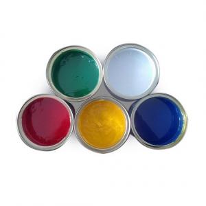
Component Liquid Thermal Curable Marking Ink Solder Mask Two Packs PCB Marking Ink
Brand Name:NUOJINSEN
Certification:ROHS,SGS
Model Number:1302
Minimum Order Quantity:100kgs
Delivery Time:7-10days
Payment Terms:T/T,LC
Contact Now
Add to Cart
Active Member
Location:
Wuhan Hubei China
Address:
29th floor room 15 No.5 Commercial building B block ,the 2nd section Wuchang Fu west,No.32 Wenzhi street,Hongshan district,Wuhan city,China
Supplier`s last login times:
within 1 hours
Shipping
lt's easy to get a shipping quote! Just click the button below and complete the short form.
Get Shipping Quote
Product Details
Company Profile
Product Details
Component liquid thermal curable solder mask , two packs pcb ink
| Items | Technical features | Notes |
| Color | black | |
| Fineness | ≤8µm | 0 ~25µm Fineness gauge |
| Mixing ratio | Base/Hardener=23/2 | Weight ratio |
| Viscosity after mixing (25℃) | 250±50 dPa﹒s | VT-04F |
| Density after mixing (25℃) | 1.20 ~1.40 g/ml | |
| Screen mesh | 36 ~51T | |
| Film thickness | 18 ~22µm | After curing |
| Curing energy | 150℃ , 30 ~60min | Hot air circulation oven |
| Pot time after mixing | 24 hours | Store below 25℃ |
| Pencil hardness | ≥6H | Pencil hardness test |
| Adhesion | 100/100 | Laceration experiment |
| Resistance to molten Tin | 288℃×10secends×3times OK | IPC-SM-840D 3.7.3 |
| Environment standard | In compliance with RoHS directives | SGS testing |
| Package | Base:920 g ; Hardener:80 g | According to customer requirements |
| Base:4.6 kg; Hardener:0.4 kg | ||
| Shelf time | 6 months since the date of manufacture | Store below 25℃ in dark |
| Items | Technical features | Notes |
| Color | White , Black | |
| Fineness | ≤8µm | 0 ~25µm Fineness gauge |
| Viscosity (25℃) | 280±20dPa﹒s | VT-04F |
| Density (25℃) | 1.20 ~1.40 g/ml | |
| Screen mesh | 90 ~120T | |
| Film thickness | 12 ~16µm | |
| Curing energy | 1500 ~2000 mJ/cm2 | The effective value through the polyester film |
| Pencil hardness | ≥4H | Pencil hardness test |
| Adhesion | 100/100 | Laceration experiment |
| Resistance to molten Tin | 260±5℃×10secends×3times OK | IPC-SM-840D 3.7.2 |
| Environment standard | In compliance with RoHS directives | SGS testing |
| Package | 1.0kg/bucket , 10kg/box | According to customer requirements |
| Shelf time | 6 months since the date of manufacture | Store below 25℃ in dark |
It is a solder mask printed by mesh and then heat-curing. After membranization, the coating is resistant to the damage from solder and chemical, print the single side or two sides of the circuit board while local solder. In order to give full play to its advantage, the detailed operation as below:
1. Making the mesh, use the mesh of 18T~36T and the squeegee of 65°— 70°.
2. Stir the gel equally. The viscosity of the gel is about 600-900ps. If you need to dilute the gel, please choose thinner special for the gel developed by us.
3. When printing, please try best to make the coating thicker to 400um or more.
4. Curing condition, two side circuit board, 150°C*3-5 minutes for the first side printing, and 150°C*18-30minutes for the second side printing.
5. Before tin solder, please check the coating with air bubble or not, please check the circuit board about leak printing. The tin stove is 260-3000°C,immerse soldering time is 3 seconds, air knife is 350-1000°C,the pressure of the air knife is 4.0-5.0kg.
6. Protect the gold fingers and gold plating position, after printing, the coating must be thicker than 350um.
7. Curing condition: 150°C*15-25minutes
Note:the thicker coating printing, the longer curing time, the better thermostability. If the coating is pull-out or melted during the soldering, please extend the curing time to 5-10 minutes. Used in protect gold finger when PCB spray-tin through the tin stove well as ware-soldering. The information above is just for reference, the actual operation depend on the environmental condition and different operating methods. The detailed operation, please contact the supplier.
Attention:
1. The base and hardner should be mixed according to the ratio and stired throughly before using.
2. We will offer you special diluent or DPM if the ink need dilute.
3. The values above are based on experients in our lab.Experients need to be carried out in order to get proper using condition.
Our company:
Hubei Nuojinsen Technology Co.,Ltd ,after years of unremitting efforts,Combined with foreign advanced technology and process,Production of PCB ink has reached the technical level, conforms to the requirement of RoHS environmental protection directive, with excellent quality and excellent service is deeply trusted by customers.
Company passed the ISO9001 quality standard certification and ISO
14000 environment system certification, is the national high and new technology enterprise. Company has
achieved many honors, including: the Chinese photographic society
of professional committee of the radiation curing, deputy director
of the unit,the ninth national committee, deputy director of the
printed circuit branch of unit, the national standardization
technical committee, deputy director of the unit printed circuit
boards, printed circuit industry in China in the second session of
"nation" brand enterprise, Hubei in 2015 advanced units of
ecological construction and environmental protection, etc.Companies
always adhere to the science and technology as the first
productivity. Enterprise technology center in Wuhan city, the
company has built in Wuhan city, and form a complete set of PCB ink
research and development of engineering technology research center,
two platform, and lead to make the printed circuit with marking ink
and the printed circuit using resistance solder "two important
industry standards. The company's flagship product, solder resist
ink (solder mask) series of products have been American UL safety
certification.

Component Liquid Thermal Curable Marking Ink Solder Mask Two Packs PCB Marking Ink
Inquiry Cart
0