10x10mmt Superconducting Thin Monocrystalline Substrate Terbium Gallium Garnet For Laser Device
Brand Name:zmkj
Model Number:TGG Wafers
Minimum Order Quantity:10pcs
Delivery Time:3-4weeks
Payment Terms:T/T, Western Union, MoneyGram
Place of Origin:china
Contact Now
Add to Cart
Verified Supplier
Location:
Shanghai Shanghai China
Address:
Rm5-616,NO.851,Dianshanhu road; Qingpu area;shanghai city//201799
Supplier`s last login times:
within 38 hours
Shipping
lt's easy to get a shipping quote! Just click the button below and complete the short form.
Get Shipping Quote
Product Details
Company Profile
Product Details
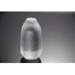
10x10mmt Terbium gallium garnet (TGG)crystals substrate wafer for laser device
Product Type: Terbium gallium garnet (TGG) crystal substrateProduct Description:TGG crystal with a large magneto-optical constants, low optical loss, high thermal conductivity and high laser damage threshold, widely used YAG, Ti-doped sapphire and other multi-stage amplification, ring, seed injection lasers. Faraday rotator is used to produce the best isolator optical materials for wavelength of 400-1100nm (not including 470nm-500nm). TGG Faraday rotator by a crystal rod and a special designed magnet. Magneto-optical material through the polarization direction of the light beam in the magnetic field deflects the direction of the deflection direction of the magnetic field only, the beam propagation direction.Optical isolator consists of a 45 ° deflection of the optical device and a pair of polarizers placed in suitable composition, which the beam in one direction only through, while blocking the reverse-propagating light beams.Technical parameters:
| Formula | Tb 3 Ga 5 O 12 |
| Lattice constant | a = 12.355 |
| Growth method | Czochralski method |
| Density | 7.13g/cm 3 |
| Mohs hardness | 8.0 |
| Mp | 1725 °C |
| Index of refraction | 1.954 at 1064nm |
| Temperature Coefficient | 9.4x10 -6 °C -1 |
| Verdet constant | 0.12min / O e. Cm at 1064nm |
Specifications:
Crystal element standard sizes:
Crystal Orientation: <111> within 5 degrees;
size: < dia100x200
Wavefront Distortion: <1/8 wave total (measured at 633nm);
Tolerance: Diameter: +0.00 mm/-0.05mm; length: ± 0.2mm;
Chamfer: 0.13mm (+0.00 mm,-0.08mm) at 45 ° ± 5 °
Note: You can provide special sizes according to customer needs and the direction of the substrate.
Standard Packaging:1000 clean room, clean bags 100
Applications
Read before inquiry:
1. If you want to customize,you need to tell me what types do you
need. Such as YAG,TGG,GGG and GAGG etc. And the materials, growth
direction, related parameters and what you will use it for are also
very important information we need to know.
2.There are many kinds of products in our products. The parameters of each product are different. If you want to know any crystal materials, we can provide detailed information. For you to choose.

10x10mmt Superconducting Thin Monocrystalline Substrate Terbium Gallium Garnet For Laser Device
Inquiry Cart
0