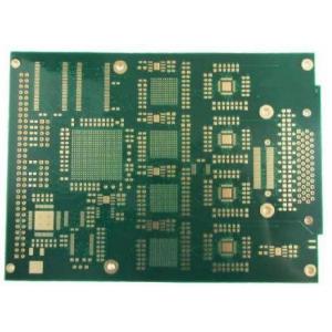
ITEQ 8 Layer PCB Assembly Services 2.0oz Copper Thickness Durable For Automobile
Brand Name:China chao sheng
Certification:ISO/UL/RoHS/TS
Model Number:CSPCB1515
Minimum Order Quantity:1PCS
Delivery Time:15-18day
Payment Terms:T/T, Western Union
Contact Now
Add to Cart
Active Member
Location:
Hong kong Hong kong China
Address:
Huishang Building, 19-128 Nathan Road, Yau Tsim Sha Tsui, Yau Tsim, Hong Kong
Supplier`s last login times:
within 48 hours
Shipping
lt's easy to get a shipping quote! Just click the button below and complete the short form.
Get Shipping Quote
Product Details
Company Profile
Product Details
Description by Manufacture
Supplier: Shenzhen Grande Electronic
Project: EDM Machine PCB Layout 8 Layers-Shenzhen Grande
Software: PADS
Layers: 8
Features:
1, Various machine interfaced.
2, Equal-length for high speed traces.
Pin number: 5600 pins
Lead time: 10 days
【Description】
PCB layout Features:
1, Huge board with perfect layout
2, Various machine interfaced, equal-length for high speed traces
PCB Fabrication:
Layers: 2
Size: 261*128*1.6mm
Surface Treatment: Im Au
Material: FR-4/HTg170, 1oz finished copper
Impedance Control Tolerance: +/-10%
Others: 4/4mil, Via:8mil
Printed circuit board (pcb) and PCBA products
Communication terminal, communication station, electronic
communication, optical fiber, optical module, communication
equipment, communication instrument, computer, household appliance,
testing equipment, testing instrument, instrument, SD card, SG
card, mobile phone, computer, various antennas, cars, music
Equipment, playback equipment, banking equipment, medical
instruments, medical equipment, medical equipment, aerospace,
aviation, military, LED, OLED, OLCD power control power supply,
industrial power supply, communication power supply, automotive
power supply, office equipment, digital
products,computers,etc.Applications;
Flexible circuit board (FPC) and FPCA product areas
CD, hard disk, printer, fax machine, scanner, sensor, mobile phone,
connector, module, walkie-talkie antenna card, high-end camera,
digital camera, laser head, CD, medical, instrumentation, drive,
automotive instrumentation, medical instrument, Medical equipment,
banking equipment, industrial instruments, LED light bars,
military, aviation, aerospace, defense and other high-tech
products, of which more than 70% of the products are exported to
Europe, America, Europe, Central Europe, Western Europe, Southeast
Asia, Asia-Pacific and other countries and area.
1: Medical Bluetooth module motherboard
2: Halogen-free FR-4 TG180, inner and outer copper thickness 35um, minimum line width line
spacing 3/3mil, hole ratio 10:1, minimum hole 0.10mm, blind hole
buried hole, immersion gold, red solder resist, white
3: The board thickness is 1.60mm,
4: blind hole, resin plug hole + plating hole
Printed Circuit Boards are 94V0 compliant, and adhere to IPC610
Class 2 international PCB
Standard.
Quantities range from prototype to volume production.
100% E-Test
PCB, FPC process production capability
| Technical ltem | MassProduct | Advanced Technology | |||||
| 2016 | 2017 | 2018 | |||||
| Max.Layer Count | 26L | 36L | 80L | ||||
| Through-hole plate | 2~45L | 2~60L | 2~80L | ||||
| Max.PCBSize(in) | 24*52" | 25*62" | 25*78.75" | ||||
| The layer number of FPC | 1~36L | 1~50L | 1~60L | ||||
| Max.PCBSize(in) | 9.8"*196" | 9.8"*196" | 10"*196"Reel to reel | ||||
| Layeredplatelayer | 2~12L | 2~18L | 2~26L | ||||
| Max.PCBSize(in) | 9"*48" | 9"*52" | 9"*62" | ||||
| Combination of hard and soft layers | 3~26L | 3~30L | 3~50L | ||||
| Interconnect HDI | 5+X+5Interconnect HDI | 7+X+7Interconnect HDI | 8+X+8,Interconnect HDI | ||||
| HDI PCB | 4~45L | 4~60L | 4~80L | ||||
| Interconnect HDI | 3+20+3 | 4+X+4Interconnect HDI | 4+X+4,Interconnect HDI | ||||
| Max.PCBSize(in) | 24"*43" | 24"*49" | 25"*52" | ||||
| Material | FR-4 Rogers | FR-4 Rogers | FR-4 Rogers | ||||
| Base material | Halogenfree,LowDK | Halogenfree,LowDK | Halogenfree,LowDK | ||||
| Build-up Material | FR-4 | FR-4 | FR-4 | ||||
| BOard,Thickness(mm) | Min.12L(mm) | 0.43 | 0.42~8.0mm | 0.38~10.0mm | |||
| Min.16L(mm) | 0.53 | 1.60~8.0mm | 0.45~10.0mm | ||||
| Min.18L(mm) | 0.63 | 2.0~8.0 | 0.51~10.0mm | ||||
| Min.52L(mm) | 0.8 | 2.50~8.0mm | 0.65~10.0mm | ||||
| MAX(mm) | 3.5 | 10.0mm | 10.0mm | ||||
| Min.CoreThickness um(mil) | 254"(10.0) | 254"(10.0) | 0.10~254(10.0mm) | ||||
| Min.Build up Dielectric | 38(1.5) | 32(1.3) | 25(1.0) | ||||
| BaseCopperWeight | Inner Layer | 4/1-8 OZ | 4/1-15 OZ | 4/1-0.30mm | |||
| Out Layer | 4/1-10 OZ | 4/1-15 OZ | 4/1-30 OZ | ||||
| Gold thick | 1~40u" | 1~60u" | 1~120u" | ||||
| Nithick | 76~127u" | 76~200u" | 1~250u" | ||||
| Min.HOle/Land um(mil) | 150/300(6/12) | 100/200(4/8) | 100/200(4/8) | ||||
| Min.Laser via/landum(mil) | 60/170(2.4/6.8) | 50/150(2/6) | 50/150(2/6) | ||||
| Min. IVH,Hole size/landum(mil) | 150/300(6/12) | 100/200(4/8) | 100/200(4/8) | ||||
| DieletricThickness | 38(1.5) | 32(1.3) | 32(1.3) | ||||
| 125(5) | 125(5) | 125(5) | |||||
| SKipvia | Yes | Yes | Yes | ||||
| viaoNhie(laserviaon BuriedPTH) | Yes | Yes | Yes | ||||
| Laser Hole Filling | Yes | Yes | Yes | ||||
| Technicalltem | Mass Product | Advanced Technolgy | |||||
| 2017year | 2018year | 2019year | |||||
| Drill hole depth ratio | ThroughHole | 2017year | .40:1 | .40:1 | |||
| Aspet Ratio | Micro Via | .35:1 | 1.2:1 | 1.2:1 | |||
| Copper Filling Dimple Size um(Mil) | 10(0.4) | 10(0.4) | 10(0.4) | ||||
| Min.LineWidth&space | lnner Layer um(mil) | 45/45(1.8/1.8) | 38/38(1.5/1.5) | 38/38(1.5/1.5) | |||
| Plated Layer um(mil) | 45/45(1.8/1.8) | 38/38(1.5/1.5) | 38/38(1.5/1.5) | ||||
| BGAPitch mm(Mil) | 0.3 | 0.3 | 0.3 | ||||
| Min.PTH Hole ring um(mil) | 75(3mil) | 62.5(2.5mil) | 62.5(2.5mil) | ||||
| Line Width Control | ∠2.5MIL | ±0.50 | ±0.50 | ±0.50 | |||
| 2.5Mil≤L/W∠4mil | ±0.50 | ±0.50 | ±0.50 | ||||
| ≦3mil | ±0.60 | ±0.60 | ±0.60 | ||||
| Laminated structure | Layer by layer | 3+N+3 | 4+N+4 | 5+N+5 | |||
| Sequential Build-up | 20L Any Layer | 36L Any Layer | 52L Any Layer | ||||
| Multi-layer overlay | N+N | N+N | N+N | ||||
| N+X+N | N+X+N | N+X+N | |||||
| sequential Lamination | 2+(N+X+N)+2 | 2+(N+X+N)+2 | 2+(N+X+N)+2 | ||||
| Soft and hard bonding | 2+(N+X+N)+2 | 2+(N+X+N)+2 | 2+(N+X+N)+2 | ||||
| PTH filling process | PTH resin plug hole + plating fill Electroplated hole/copper plug hole | PTH resin plug hole + plating fill Electroplated hole/copper plug hole | PTH resin plug hole + plating fill Electroplated hole/copper plug hole | ||||


ITEQ 8 Layer PCB Assembly Services 2.0oz Copper Thickness Durable For Automobile
Inquiry Cart
0